We can use the same STM32duino platform by changing the following:-
I just only change. Following in stm32.h
\IDE\hardware\Arduino_STM32\STM32F1\system\libmaple\stm32f1\include\series
#if STM32_F1_LINE == STM32_F1_LINE_PERFORMANCE
# ifndef STM32_PCLK1
# define STM32_PCLK1 54000000U // << from 36000000
# endif
# ifndef STM32_PCLK2
# define STM32_PCLK2 108000000U // << from 72000000
Tested hardware:
I/O = Work
Serial123 = Work
Timer 1234 = Work
SPI 1/2 = Work
I2S = not done
You may need to adjust the delay(100); Because it blink Faster.
I still not check the delay lib yet.
———————————————————————————————————-
Have fun.!
I have ordered some boards from taobao via yoybuy, but I am still awaiting confirmation of the order.
Re: code changes
OK. I think we need to move those defines into the Variants folder or into boards.txt, or perhaps read the cpu frequency defined value and use that to switch those values.
What we really need to now is whether USB works at 108mhz clock ?
In the variant, the BOARD_RCC_PLLMUL is clearly defined as RCC_PLLMUL_9 for the MapleMini.
It is located in Arduino_STM32/STM32F1/variants/maple_mini/wirish/boards_setup.cpp
By creating a new GD32 variant, it will be easy to define the BOARD_RCC_PLLMUL to RCC_PLLMUL_11.
Because I think without that, only the above #define won’t be not enough…
I suspect there will be quite a few changes required, including some changes to the core, and to either move things to the variant or add more #defines.
Also, the delay() functions are hard coded loops of nops which assume 72Mhz, so that would need to be changed as well.
I suspect there will be quite a few changes required, including some changes to the core, and to either move things to the variant or add more #defines.
Also, the delay() functions are hard coded loops of nops which assume 72Mhz, so that would need to be changed as well.
You are probably right.
Actually, what I really need to do is to pull all the cores into their own individual repo’s and re-attach as sub-modules, but I don’t want to loose the commit history (which would get hidden if I did this).
It is possible to retain the history, and move a folder to its own repo, but from what I’ve read its not a simple process, and stands the chance of screwing up the repo and removing files if I screw up.
One other option is to move this stuff to my other Github account of STM32duino, which I created when I setup this forum.
But I don’t really have time to do this level of re-organisation at the moment.
I the programming manual for the GD32 and in terms of USB, it will work when the device is running at 108Mhz
The usb clock prescaler is now 2 bits instead of 1 bit, so that a divider of 2.5 can be selected, which is what is required to operate at 108Mhz
USBPS USB clock prescaler selection
Set and reset by software to control the USB clock prescaler value. The USB clock
must be 48MHz. These bits can’t be reset if the USB clock is enabled.
00: (CK_PLL / 1.5) selected
01: CK_PLL selected
10: (CK_PLL / 2.5) selected
11: (CK_PLL / 2) selected
It also appears to be able to operate at 48, 72 and 96Mhz.
But this definately means we need to copy the STM32F103 core and make a new GD32F103 core to start accomodating this stuff.
I can not test USB boot loader untill i re-solder BOOT1 pin.
overall. It works by #define.
RTC = Work.
I put IDE in 2 Folder. For STM32 and GD32.
But you need to change working folder everytime you switch STM32 or GD32.
Roger,
Hope you get board soon. You will have fun.
I think you may look for GIGADEVICE co-promotion now.
Thanks.
I did not pay for express postage, so I think it will be several weeks before the boards arrive.
Re: GD32F1 folder
I need to make a new folder for this in the repo.
I can do it now, but I can’t test it.
Re: Boot1
I’m not sure what you mean.
If you can upload a sketch, you can upload a bootloader, even if you need to run stm32flash on the command line
I think you may look for GIGADEVICE co-promotion now.
I think I need to wait until we have some boards ;0)
I think you may look for GIGADEVICE co-promotion now.
So in the longer term, it may be possible to leverage the work that @sheepdoll has done around using STM’s HAL SPL
But I think to get us up and running more quickly, its probably expedient to just copy the STM32F1 core folder and make some changes to get the basics working.
The rest can come in time if there is sufficient interest.
At 108Mhz the speed of this device is entering Teensy territory, albeit no FPU.
I will be interesting to see if the displays like the ILI9341 will run at SPI DIV2 i.e 56Mhz.
So if I can make a new core ( which i suspect is just a slightly modified copy of the F103 core), Im pretty sure I will be reselling these boards, as I really dont need 20 of them;-)
I will also need to get the Bootloader to work with this board, but I’m hoping its a fairly minor change.
Well, this is always assuming that the USB has that 1.5k pullup, and if not… I will be doing a lot of soldering ![]()
I found the programming manual for the GD32 and they have added another bit to the USB PLL divider – previously it was either DIV 1.5 or DIV 1 i.e so you could run the STM32 on either 72Mhz / 1.5 = 48Mhz USB or run the STM32 on 48 Mhz and used DIV 1
On the GD32 it has 2 bits (4 combinations) and they added dividers for something like 96Mhz and for 108Mhz
So we just need to set one more bit in the PLL control register.
But of course adding a bit in the middle of the PLL reg has probably displaced some other bits upwards, so I’m a bit surprised the OP’s board was working at all
But overall, I do think that USB is supposed to work at 108Mhz main clock.
PS. I didnt realised that the flash control stuff was also different, but like you say, its probably just some small changes.
My boards are not supposed to be here until mid Sept, so it will be a while before I can test out any of this stuff.
Seems you getting a lot of GD board. I try to get the GD32F103ZET6.
But difficult to find.
I already get this STM32F103ZET6 PCB.
http://world.taobao.com/item/5204590784 … 7Zp#detail
I am buying the GD32F103ZET6 sample. But There is no stock in Taobao.
Some of them ask > Project information / company name before quote.
Seems quite new for GD32F103ZET6.
Thanks,
Jackson009
They have included a USB to serial connector (I guess as a free / bonus item).
It came tripple rapped through YoyBuy, which looks like it really pushed up the postage costs. I weighed the boards and and they came to 100g but I think YoyBuy said that total weight was 400g, so it was 300g of packaging.
Well I’m sure its not, but I do have 2 packages of board coming from YoyBuy (due to my mistake when ordering) so perhaps the next lot will be in a box etc. Otherwise I’m struggling to see how they think it ways 400g.
Anyway.
I’ve not had time to do much apart from look at the board using STM’s Serial uploader and it reports as 64k. I’ll need to check if its actually got more than 64k flash i.e like the STM32F103C version.
As a quick test, I thought I’d try to upload the new bootloader, and guessed the Led is on PC13 – which it is, because the bootloader does flash the LED (a lot faster than it should be flashing).
However the device is not appearing on USB at all, not even as an unrecognized device before I even flashed the bootloader – this is a bit of a concern, as most times if something is plugged into the USB, I at least get an known device message.
There seem to be some 2 x 220 ohm resistors near the USB connector, but its hard to see what they are connected to. I’m hoping they are the USB D+ and D- but 220 Ohms seems a bit high for USB resistors, as they are normally 22 ohms
Anyway. I’ll take a more detailed look this evening
22R ” ” 220?
I am not sure which board you get. Pls see the schematic of the board i have.
There are 22Ohm resister on USB connector.
Thanks,
Jackson009
I checked again and I think “220” on the resistors means 22 x 10 ^ 0 i.e 22 x 1 = 22
But. The board does not look like USB D+ is pulled high by a 1.5k resistor, So the bootloader will not work, as it assumes that D+ will float to Vcc (3.3V when not driven by the GPIO)
The current bootloader code resets the USB like this
#define USB_DISC_BANK         GPIOA

#define USB_DISC              12
SET_REG(GPIO_CR(USB_DISC_BANK,USB_DISC),
(GET_REG(GPIO_CR(USB_DISC_BANK,USB_DISC)) & crMask(USB_DISC)) | CR_OUTPUT_PP << CR_SHITF(USB_DISC));
gpio_write_bit(USB_DISC_BANK,USB_DISC,0); /* present ourselves to the host */
volatile unsigned int delay;
for(delay = 0;delay<256;delay++);
// volatile unsigned x = 1024; do { ; }while(--x);// wait a moment
/* turn on the USB clock */
SET_REG(GPIO_CR(USB_DISC_BANK,USB_DISC),
(GET_REG(GPIO_CR(USB_DISC_BANK,USB_DISC)) & crMask(USB_DISC)) | CR_INPUT << CR_SHITF(USB_DISC)); //Sets the PA12 as floating input
I’ve had a quick look at changing the USB prescaler, and it looks like Bit 23 needs to be set, so I changed the PLL config reg to this
SET_REG(RCC_CFGR, GET_REG(RCC_CFGR) | 0B100111010000010000000000);
Pls take a look at Crystal on the board.
GD board is using the 12MHz x 9PLL = 108M.
STM32 is using. 8M x 9 PLL = 72M.
Cheers!! ![]()
Yes. I looked at the schematic.
The Crystal resonator is 12mhz. Which means the STM32 PLL settings e.g main clock of 9 x crystal, gives 108MHz instead of 72Mhz
To get USB working in the bootloader, the USB clock needs to run at 48Mhz, so it need a different divider config.
On the STM32, bit 22 of the PLL config register is the divider setting where 0 = divide by 1.5
(interestingly bit 23 on the STM32 is reserved)
On the GD32 bits 22 and 23 are the USB divider, and for 108mhz operation, the setting need to be 10.
ie bit 23 set, and bit 22 reset.
So i tried changing this in the bootloader, but USB still does not appear as a device at all on my PC.
This is a bit worrying, as most boards enumerated as an Unknown Device on Windows, even if the USB has no firmware.
I need to review what other changes you had to make to the core to get your board to work, in case i need to change more things in the bootloader.
Yes. I think thats the next step.
I’m not sure if there are any other config changes on the USB, i,e differences between the GD32 and the STM32 other than the USB clock.
I’m a bit surprised that by default it doesn’t show up on USB at all. i.e not even an unrecogised device, which makes me think something is missing in the setup or the hardware
I just only change. Following in stm32.h
\IDE\hardware\Arduino_STM32\STM32F1\system\libmaple\stm32f1\include\series
#if STM32_F1_LINE == STM32_F1_LINE_PERFORMANCE
# ifndef STM32_PCLK1
# define STM32_PCLK1 54000000U // << from 36000000
# endif
# ifndef STM32_PCLK2
# define STM32_PCLK2 108000000U // << from 72000000
I flash GD32 by USBtoSerial(CH340). All code seems to be worked fine.
I think USB boot loader is most hardest one.
Thanks,
Jackson
I don’t know if the bootloader has many timing loops that need to be changed, but I will adjust the USB reset delay loop and make its 1.5 times longer or perhaps 2x longer so that the reset delay is the same length of time.
Re: USB
I flashed via USB to Serial, but I want to get USB working, as its very useful and most people now use USB for upload and debug etc
I have more than one GD32 board so I will try another in case the one I tried has a fault on USB.
In theory it looks like I just need to change the USB PLL divider, but there may be other differences.
I think someone found a list of differences on a Russian website, so I will need to look for that.
Thanks
The USB socket on the PCB was pulled off completely just with the weight of the USB cable.
I wasnt even inserting the cable, I think the socket snapped off when I picked up the board and put it on another table while a 1m length of USB cable was still plugged in.
I didnt notice until I picked up the board again this evening.
Looking at the USB socket, the restraining points didnt show any signs of having any solder on them at all, so I think the manufacturing quality on these boards is not that good.
Fortunately, I’m getting quite good at hand soldering surface mount items, and I was able to solder it all back on again.
After I resoldered the USB connector, I checked whether this had fixed the USB, but it had not ![]()
I checked the connections of the D+ and D- pins from the cable to the GD32 and I can see the connections right the way through to the GD32 on PA11 and PA12.
So the problem is not a bad connection, it looks like its a software issue.
I’ve not had time to look at the D+ or D- lines on the scope, and to be honest I’m not sure what I would be looking for.
I will need to see if there is any information on the web about what sort of signals I should see
It doesnt seem to mention USB, in fact it does not say much really
http://www.zlgmcu.com/GigaDevice/img/GD32F103xx_en.pdf
I’ve also seen this list
(1) UART2 used DMA1_channel_6 + DMA1_channel_7 + UART_2 interrupt
(2) UART4 used DMA2_channel_3 + DMA2_channel_5 + UART_4 interrupt
(3) SPI1 used DMA1_channel_2 + DMA1_channel_3 + SPI1 Interrupt
(4) SPI2 used DMA1_channel_5
(5) SPI3 with a break
(6) PWM with a PB0, PB1, PC6, PC7
(7) ADC with the PC0, PC1, PC2, PC3
(8) several GPIO
(9) with a SysTick SysTick interrupt
(10) FLASH with the original ST library function FLASH_Unlock (), FLASH_ProgramHalfWord (), etc. FLASH can be erased and written
(11) have to use battery-powered BKP RAM memory to save the data
(12) have to use watch_dog
(13) Useful GPIO PB6, PB7 -> EXTI9_5_IRQ interrupt
other software behavior:
(1) call SCB-> VTOR remap jump table
(?? In this chip inside it is only 96bit code it) (2) to read 96bit of UID
(3) there are in the program in open ROP, and close ROP (Chip empty)
(4) of the function directly access unaligned data (STM32 support, I do not know this line does not?)
I think I found a mistake I made with the USB bootloader
I presumed that selecting the maximum PLL divider was the correct value to use, i.e I selected 2.5
USB clock prescaler selection

Set and reset by software to control the USB clock prescaler value. The USB clock

must be 48MHz. These bits can’t be reset if the USB clock is enabled.

00: (CK_PLL / 1.5) selected

01: CK_PLL selected

10: (CK_PLL / 2.5) selected

11: (CK_PLL / 2) selected
I tried changing the PLL multipler to push the GD32 up to 120Mhz, and left the USB divider set at 2.5, hence the USB clock should be the correct speed of 48Mhz, but I’m still not seeing anything at all on USB ![]()
So… I changed the PLL multiplier down to 6 x (the 12Mhz) so that the clock would be 72Mhz, i.e the same as the STM32 and changed the USB PLL bits back to 00, i.e 1.5 divider, hence USB clock of 48Mhz
However, I’m still not seeing anything on USB ![]()
I’m not entirely sure I’ve got the bit pattern correct for the RCC config reg, as when I set the PLL for x 6 i.e to make 72Mhz, the speed of the LED flash in the bootloader seemed wrong.
So I think I’m going to need to go back to first principals on the PLL and make sure the PLL for the main clock is correct eg get it running at 72Mhz, then make sure what speed the USB is running at – however I’m not entirely sure how I can measure the usb clock speed. Perhaps I can just put a scope on PA11 or PA12 and look at the waveforms
Any idea of what I should see ??
http://www.lemicro.cn/pdf/GD32%E4%B8%8E … %A2%98.pdf
Which is in chinese, so here is a google translation (apologies for the loss of formatting)
Page 1
GD32 introduce compatibility with STM32 summary
A, GD32 and STM32 similarities and differences
1. The same point
1)
Peripheral pin definition:
Same pin definitions of the same model
2) Cortex M3 core:
R1P1 kernel version STM32F103, STM32F205 kernel R2P1,
GD32 R2P1 kernel version, this kernel fixes some bug R1P1
3)
Chip internal registers,
External IP Register Address: same logical address, is mainly based on the STM32 registers and physical address,
Do positive development.
4)
Library file:
The same libraries, optimized header files need to be changed
5)
Compilation Tools:
Exactly
For example: keil MDK, IAR
6)
Model naming:
Exactly
2. The difference between the peripheral hardware
1)
Voltage range (ADC): GD32F: 2.6-3.6V
STM32F: 2.0-3.6V (external voltage)
GD32F: 1.2V (core voltage) STM32F: 1.8V (core voltage)
2)
BOOT 0 pins:
Flash runtime, BOOT0 on the STM32 can be suspended, GD32 must be outside
Section pulldown (from the Flash runtime, BOOT0 must drop down to)
3)
ESD parameters:
STM32 HBM 2KV, air mode 500V
GD32 body mode 4KV (beta 5KV), air mode 10KV (beta 15KV)
3. The internal structure of the difference
1) Start time:
GD32 start times are the same, because the GD run slightly faster, the need to extend the power of time
Configuration (2ms)
2) frequency clock:
GD32F10 series clocked at 108MHZ STM32F10 series frequency 72MHZ
3) Flash erase time: GD32 is 60ms / page, STM 30ms / page
4) FLASH capacity:
GD32 maximum capacity of 3M Byte
5) SRAM space:
GD32F103 series, GD32F105 \ 107 large-capacity SRAM 96K series
6) VB external expansion bus FSMC: GD32 100PIN configure the bus output, STM32 144PIN and above 256k
Only configure the bus output
4. Power difference (to 128k or less capacity as a reference)
1) Sleep mode Sleep:
GD32F: 12.4mA STM32F10X: 7.5mA
2) Deep Sleep Mode Deep Sleep:
GD32F: 1.4mA STM32F10X: 24uA
3) Standby mode Stand By:
GD32F: 10.5uA STM32F10X: 3.4uA
4) Run Power:
GD32F: 32.4mA / 72M STM32F10X: 52mA / 72M
LEMICRO
Beijing Link Technology Co., Ltd.
Tel: 010-82674978
http://www.lemicro.cn
Page 2
5. Internal FLASH difference
1) ISP:
Erase time differences with STM32, use the new ISP software
2) IAP:
Erase the same time, according to the word written, erased by page
3) Storage life:
10 million times rewritable, data retention more than 20 years
4) encryption features:
In addition to conventional reading and 96 prohibit ID number encryption, GD32 data write
Flash when having stored logical addresses continuous physical addresses are not contiguous properties.
Two, GD32 detailed description and analysis of the compatibility
1. System
1) Start-up crystal difference
Description
Start time, GD32 and STM32 start time is 2ms, in fact, the efficiency of GD Express, the
In ST’s HSE_STARTUP_TIMEOUT ((uint16_t) 0x0500) is 2ms, but the value of this macro definition
GD in short time more, so set this value to increase
Solution
The macro definitions:
#define HSE_STARTUP_TIMEOUT ((uint16_t) 0x0500)
Revised to:
#define HSE_STARTUP_TIMEOUT ((uint16_t) 0xFFFF)
Note: Start time macros Location:
1, in V3.X library, its start time macros are defined in the header file stm32f10x.h
(Path: \ .. \ Libraries \ CMSIS \ CM3). (Different versions of the directory where the library is also different)
2, in the previous V3.0 libraries, its start time macros are defined in the source file stm32f10x_rcc.c
(HSEStartUp_TimeOut)
(Path: \ .. \ Libraries \ STM32F10x_StdPeriph_Driver \ src).
2) Some customers use active crystal problems in GD32F103 small volume products, found to the complex in the MCU
Bit pin has been pulled to the level of 0.89V, the level can not be maintained at a high level
Description
Because some active crystal start-up time is too fast, the reset signal has not been completed due to
Solution
That is, before the active crystal input and ground and a 30pf capacitor
3) GD32 MCU clocked at 108MHz support high-performance, code transplantation takes note
Description
GD32 increased through internal chip cache to improve the speed of code execution under the same operating frequency, bringing
A high performance experience.
Solution
Therefore, if the code to be useful for loop or while loop to make precise timing, timing will be made
In code execution speed leaving the cycle time becomes shorter. Use Timer timer is not affected.
4) GD32F105 / 107 Series MCU is configured to 108MHz What is the difference
Description
By Clock configuration register (RCC_CFGR), the first 21:18 bits
PLLMUL [3: 0], and then in conjunction with article 29 PLLMUL [4] composed of five bit field to determine the PLL frequency multiplier
Coefficient, that configuration to define the PLL multiplication factor by software, and the PLL output frequency is definitely not
Exceed the highest frequency (108MHz).
LEMICRO
Beijing Link Technology Co., Ltd.
Tel: 010-82674978
http://www.lemicro.cn
Page 3
2. Internal Flash
1) Chip Set read protection Usage
Description
Because Flash is GD’s own patented technology, STM’s Flash is provided by third parties, so GD
The Flash and Flash STM’s slightly different. GD president erase time point
Solution
After finished KEY sequences need to read this bit, confirm key has taken effect.
So, here should be inserted
While ((FLASH-> CR & 0x200)!); // Wait OPTWRE
Or can simply insert two NOP.
__NOP ();
__NOP ();
In ST libraries, only
FLASH_Status FLASH_EraseOptionBytes (void)
FLASH_Status FLASH_ProgramOptionByteData (uint32_t Address, uint8_t Data)
FLASH_Status FLASH_EnableWriteProtection (uint32_t FLASH_Pages)
FLASH_Status FLASH_ReadOutProtection (FunctionalState NewState)
Four functions need to be modified.
2) IAP In-Application Programming
Description
Because of its own flash access timing of 0, with STM32 in the Flash Erase and Program on GD32
There is a difference, GD32’s Erase and Program time is slightly longer than the STM32 some, it is recommended to Erase
Program time and make changes.
Solution
The macro definition
#define EraseTimeout
((Uint32_t) 0x000B0000)
#define ProgramTimeout
((Uint32_t) 0x00002000)
Revised to:
#define EraseTimeout
((Uint32_t) 0x000FFFFF)
#define ProgramTimeout
((Uint32_t) 0x0000FFFF)
Note: Erase and Program time macros are defined in the source file stm32f10x_flash.c
(Path: \ .. \ Libraries \ STM32F10x_StdPeriph_Driver \ src)
3) with IAR download configuration
Solution
In mass production, when the first will program a USB boot, in the rear of the boot automatically run
Bit machine software programming applications. If the boot program does not run automatically you will need to re-plug a
Secondary power supply. Cause some trouble to the production. The reason is that the program does not run automatically if the program settings
Read protection if need to wait FLASH_CR first 9 [OPTWRE] bit is 1. If there is no set of words continues
Execution error occurs. Due to the slow speed of execution ST, program execution time to read FLASH_CR register
This bit is already set, GD relatively fast execution speed, the program runs to this time have not set this bit, because
This requires FLASH_ReadOutProtection function inside to add some polling this bit is 1 or plus one
Some delay.
LEMICRO
Beijing Link Technology Co., Ltd.
Tel: 010-82674978
http://www.lemicro.cn
Page 4
3. ISP programming software
1) ISP programming, the programming software is recommended to use official
Description
GD32 STM32 chip flash with a difference
Solution
It is recommended to download the latest version www.mcuisp.com MCUISP. GD32 also has a special addition
Programming software (GigaDevice MCU ISP Programmer)
You can download the http://bbs.21ic.com/gd32 forum.
If you use a homemade ISP or offline programming software, to achieve fully compatible with ST and GD proposed changes
The following parameters.
1, page erase timeout period increased to 300ms, full chip erase timeout period increased to 3s left
Right.
2, the word programmed timeout period increased to 2ms, page programming, etc. timeout increased to 300ms.
I / O ports
1)
IO port external interrupt usage
Description
During the shutdown, if there is an external pin level change, after using the IMR will immediately break into the open
The interrupt service routine. Theory is open before the interruption, regardless of whether there is pin level change, are not shadow
The interrupt response to turning on.
Solution
So the solution is rising or falling edge detection by disabling switch interrupt register, can not make
With IMR mask register. Procedures are as follows:
EXTI-> FTSR & = EXTI_Line3;
// Close edge detection to achieve close disruption
Purpose, falling use FTSR register, the rising use RTSR register
EXTI-> PR = EXTI_Line3;
EXTI-> FTSR | = EXTI_Line3;
2) In the standby mode, PA8 pin special settings
Description
In the case of low-power, PA8 MCU will be internally set to
PA8 of MCU internal frequency multiplexed output, when ultra-low power settings need to float
Solution
In standby mode, PA8 suspended without
3) Low power consumption must be taken
Description
In the case of the use of low-power, the software all ports (AF) clock turned off, regardless of whether the port.
4) When burst impact pin
Description
After entering the required interrupt disable interrupts
LEMICRO
Beijing Link Technology Co., Ltd.
Tel: 010-82674978
http://www.lemicro.cn
Page 5
4. Timer
1) Timer input capture mode requires software clears the interrupt
Description
STM timer input capture mode by default can clear the hardware interrupt, GD more stringent requirements for the configuration,
Done by software interrupts
Solution
Software Removal flag
2) Timer pulse counting mode is set up
Description
Usage difference timer
Solution
Pulse counting mode, the load value must be set larger than the expected value, or do not count
If the reload value in the ST is not set (initially 0) when, CNT can normally count.
On GD if the reload value is not set to 0 to maintain the initial time, because the reload value to zero, even
To a pulse will cause all of the registers are reset and thus can not properly counted.
Model
GD32F1 series MCU (Flash 256KB and above models)
3) TIM, ADC module
Description
Trigger signal width Timer, ADC module requirements
Solution
Since the internal high-speed and low-speed two peripheral bus, Timer, ADC module and other commonly used peripherals
Both buses. GD32F103 / 101 series Flash 128KB and following models, Timer, ADC, etc.
Conditions module identifies the trigger signal is a trigger signal width greater than the width where the bus module clock.
5. Serial USART
1) USART continuously transmitted data byte idle position
Description
Inter byte idle position
Solution
For general communications, it will not be affected, only general in the communication have a special agreement, will
Produce inaccurate data
Therefore, the specific circumstances, to modify the program
6. I2C bus
1) hardware I2C special configuration
Description
GD’s I2C relatively STM’s is less a flag
Solve
Method
1, change the definition of the macro address
#define
I2C_EVENT_SLAVE_TRANSMITTER_ADDRESS_MATCHED
((Uint32_t) 0x00060002)
#define
I2C_EVENT_MASTER_TRANSMITTER_MODE_SELECTED
LEMICRO
Beijing Link Technology Co., Ltd.
Tel: 010-82674978
http://www.lemicro.cn
Page 6
((Uint32_t) 0x00070002)
2, the hardware I2C after the meeting to send 7bits address from the machine is complete, the slave has not had time to identify. (See Customer
Applications)
We can send after completion 7bits add a delay, so that the machine fully identify:
I2C_Send7bitAddress (I2C1, EEPROM_ADDRESS, I2C_Direction_Transmitter);
ʱ??
int i = 0xfff;
while (i -);
ʱ??
3, the detection ADDR function can not be used I2C_CheckEvent, because he will clear ADDR, you can use
I2C_GetFlagStatus functions.
It is to
while (! I2C_CheckEvent (I2C1,
I2C_EVENT_MASTER_TRANSMITTER_MODE_SELECTED));
Changed while (I2C_GetFlagStatus (I2C1, I2C_FLAG_ADDR)!);
4, there is a step on the rigor of programming, with the STM want more than that we are first Clear_ACK, then Clear_ARRD.
7. ADC acquisition
1) ADC Sampling Settings
Description
ADC start
Solution
Threefold
1. When ADON = 0 after writing 1, the need to wait for some time t_WAIT, if the ST libraries words
Just behind ADC_CMD plus delay 20us so.
2. If the interrupt obtain sampling data, the need for software clears the interrupt.
8. SDIO
1) 1 bit bus mode and 4 bit bus mode configuration SDIO DAT 3 pin of
Description
1, SDIO at 1 bit bus mode, DAT 3 pin is low, this will lead into the SD Card
The SPI mode.
Reason: Failed to initialize the main reason is because GD32 chip SDIO port presence of DAT3
BUG.
2, in the 4 mode, by the above method, the program can properly initialized, but can not read and write properly SD
Card.
Reason: Because DAT3 mouth in front of a push-pull output has been configured, so in four modes, not
Under normal reading.
Before calling 4 mode, the port is configured to DAT3 complex problems can be solved using the push-pull input.
Solution
1, 1 bit bus mode solution: It is recommended before SDIO enabled first SDIO DAT 3
pin configured as push-pull outputs, and to set to high, the SDIO DAT 3 pin remains high
Flat to
2, 4 bit bus mode Solution: Before calling four modes of the configured port DAT3
Multiplexed output to solve the problem.
LEMICRO
Beijing Link Technology Co., Ltd.
Tel: 010-82674978
http://www.lemicro.cn
Page 7
2) immediately after the burn program can read and write properly SD card, power off and on again, SD card initialization fails, you need to manually
Reset once after normal
Description
In some SD card, GD32 off and on again, it will cause the clock signal on the SD card is not normal, resulting in
SD card to send commands to fail.
Solution
In the program, open the SD card clock, increase small delay, to ensure SD card clock signal is stable.
This delay added places: in sdcard.c (ie, SDIO configuration file), then SD_Error
SD_Init (void) This function is found SDIO_DeInit (); to add a delay in the back.
RCC_AHBPeriphClockCmd (RCC_AHBPeriph_DMA2, ENABLE);
SDIO_DeInit ();
ʱ??
int i = 0xffff;
while (i -);
ʱ??
10. USB
A. USB_OTG
1) When customers use the STM32 DFU original project points to note
Solution
Decide
Square
France
1, in usb_istr.c, add the statement as shown in red
for (i = 0; i <8; i ++) EP = _GetENDPOINT (i);
for (i = 0; i <8; i ++)
_SetENDPOINT (I, EP & 0x7070);
2, in usb_conf.h in red font in the following figure modify statement
#if
defined (STM32L1XX_MD)
||
defined (STM32L1XX_HD) ||
defined (STM32L1XX_MD_PLUS)
#define INTERN_FLASH_SECTOR_ERASE_TIME
100
#define INTERN_FLASH_SECTOR_WRITE_TIME
104
#else
#define INTERN_FLASH_SECTOR_ERASE_TIME 100
#define INTERN_FLASH_SECTOR_WRITE_TIME 100
3, the firmware library stm32f10x_flash.c use attachments to be replaced.
4, the software needed to read protect bit selected using FLASH_Unlock (); function
int main (void)
ʱ??
#if defined (USE_STM32L152D_EVAL)
FLASH_Unlock ();
FLASH_ClearFlag (FLASH_FLAG_OPTVERRUSR);
#endif
FLASH_Unlock ();
FLASH_ReadOutProtection (ENABLE);
FLASH_Lock ();
LEMICRO
Beijing Link Technology Co., Ltd.
Tel: 010-82674978
http://www.lemicro.cn
Page 8
2) some USB compatibility
Solution
Decide
Square
France
1. Some U disk has three endpoints, leading to an array of cross-border Itf_Desc be cleared, so the host does not recognize the device
Types of. USBH_conf.h file USBH_MAX_NUM_ENDPOINTS defined by 2 can be changed to 3
Will: #define USBH_MAX_NUM_ENDPOINTS
2
Read: #define USBH_MAX_NUM_ENDPOINTS
3
2. In the endpoint interrupt handler USB_OTG_USBH_handle_hc_n_In_ISR, for NAK interrupt,
V1.0.0 version of the process is as follows:
else if (hcint.b.nak)
ʱ??
if (hcchar.b.eptype == EP_TYPE_INTR)
ʱ??
UNMASK_HOST_INT_CHH (num);
USB_OTG_HC_Halt (pdev, num);
CLEAR_HC_INT (hcreg, nak);
ʱ??
else if ((hcchar.b.eptype == EP_TYPE_CTRL) ||
(Hcchar.b.eptype == EP_TYPE_BULK))
ʱ??
/ * Re-activate the channel * /
hcchar.b.chen = 1;
hcchar.b.chdis = 0;
USB_OTG_WRITE_REG32 (& pdev-> regs.HC_REGS [num] -> HCCHAR, hcchar.d32);
ʱ??
pdev-> host.HC_Status = HC_NAK;
ʱ??
The version V2.1.0 NAK process is as follows:
else if (hcint.b.nak)
ʱ??
if (hcchar.b.eptype == EP_TYPE_INTR)
ʱ??
UNMASK_HOST_INT_CHH (num);
USB_OTG_HC_Halt (pdev, num);
ʱ??
else if ((hcchar.b.eptype == EP_TYPE_CTRL) ||
(Hcchar.b.eptype == EP_TYPE_BULK))
ʱ??
/ * Re-activate the channel * /
hcchar.b.chen = 1;
hcchar.b.chdis = 0;
USB_OTG_WRITE_REG32 (& pdev-> regs.HC_REGS [num] -> HCCHAR, hcchar.d32);
ʱ??
pdev-> host.HC_Status [num] = HC_NAK;
CLEAR_HC_INT (hcreg, nak);
LEMICRO
Beijing Link Technology Co., Ltd.
Tel: 010-82674978
http://www.lemicro.cn
Page 9
ʱ??
The only difference is CLEAR_HC_INT (hcreg, nak) location in the V1.0.0 release and for CTRL
BULK endpoint NAK interrupt is not cleared NAK, our chips will therefore generate multiple IN transfer request, guide
Cause data transmission errors. Transfer to normal after the wording be changed to V2.1.1. (Note that in V2.1.0 is the number HC_Status
Group, in V1.0.0 is a single data directly if you want to get rid of the copy back [num])
B.
USB peripherals operating frequency restrictions
Description
It has the lowest operating frequency requirement is APB1 the divided clock must be greater than 12MHz, such as
HCLK is 56MHz, APB1 maximum frequency coefficient 4,56 / 4 = 14MHz, to work properly.
11. SPI
1) Input and output configuration requirements (STM32 not need such a request)
Solve
Method
GD32 When using SPI, IO configuration must be strictly observed master from the input and output mode configuration,
STM32 is no such requirement, the relevant code is as follows:
Host mode IO configuration (host to SPI for example):
GPIO_InitStructure.GPIO_Mode = GPIO_Mode_AF_PP;
GPIO_InitStructure.GPIO_Speed = GPIO_Speed_50MHz;
GPIO_InitStructure.GPIO_Pin = GPIO_Pin_5 | GPIO_Pin_7;
GPIO_Init (GPIOA, & GPIO_InitStructure);
GPIO_InitStructure.GPIO_Mode = GPIO_Mode_IN_FLOATING;
GPIO_InitStructure.GPIO_Pin = GPIO_Pin_6;
GPIO_Init (GPIOA, & GPIO_InitStructure);
IO configured in slave mode (slave in SPI2 example):
GPIO_InitStructure.GPIO_Mode = GPIO_Mode_IN_FLOATING;
GPIO_InitStructure.GPIO_Speed = GPIO_Speed_50MHz;
GPIO_InitStructure.GPIO_Pin = GPIO_Pin_13 | GPIO_Pin_15;
GPIO_Init (GPIOB, & GPIO_InitStructure);
GPIO_InitStructure.GPIO_Mode = GPIO_Mode_AF_PP;
GPIO_InitStructure.GPIO_Pin = GPIO_Pin_14;
GPIO_Init (GPIOB, & GPIO_InitStructure);
3) In the GD32’s SPI clock signal, idle needs to be configured to a high level, to ensure the stability of data,
Specific code as follows: red font code
Solve
Method
SPI_InitStructure.SPI_Direction = SPI_Direction_2Lines_FullDuplex;
SPI_InitStructure.SPI_Mode = SPI_Mode_Master;
LEMICRO
Beijing Link Technology Co., Ltd.
Tel: 010-82674978
http://www.lemicro.cn
Page 10
SPI_InitStructure.SPI_DataSize = SPI_DataSize_8b;
SPI_InitStructure.SPI_CPOL = SPI_CPOL_High;
SPI_InitStructure.SPI_CPHA = SPI_CPHA_2Edge;
SPI_InitStructure.SPI_NSS = SPI_NSS_Soft;
SPI_InitStructure.SPI_BaudRatePrescaler = SPI_BaudRatePrescaler_256;
SPI_InitStructure.SPI_FirstBit = SPI_FirstBit_MSB;
SPI_InitStructure.SPI_CRCPolynomial = 7;
SPI_Init (SPI1, & SPI_InitStructure);
4) When used as a slave, in GD32, the clock signal must be an integer multiple of 8.
For example: red font code
Solve
Method
SPI_InitStructure.SPI_Direction = SPI_Direction_2Lines_FullDuplex;
SPI_InitStructure.SPI_Mode = SPI_Mode_Master;
SPI_InitStructure.SPI_DataSize = SPI_DataSize_8b;
SPI_InitStructure.SPI_CPOL = SPI_CPOL_High;
SPI_InitStructure.SPI_CPHA = SPI_CPHA_2Edge;
SPI_InitStructure.SPI_NSS = SPI_NSS_Soft;
SPI_InitStructure.SPI_BaudRatePrescaler = SPI_BaudRatePrescaler_256;
SPI_InitStructure.SPI_FirstBit = SPI_FirstBit_MSB;
SPI_InitStructure.SPI_CRCPolynomial = 7;
SPI_Init (SPI1, & SPI_InitStructure);
5) In the GD32, you can not use this bit to determine whether SPI_I2S_FLAG_BSY SPI bus data received or sent
carry out.
12. Watchdog
1) Before entering STOP mode opens the watchdog, after waking up by the RTC ALR, the program will continue to be reset it is like
Description
IWDG Reload signal inside there, KEY register write AAAA will make it pulled, over a period of time from
Move down. Before entering the STOP state will pull the bottom Reload signal remains high until exit STOP
After also remains high, then there is no way to write AAAA let Reload rising edge, but also no way to more
A new counter.
Solution
Do not Reload Before entering STOP, you can also adjust the order under the program, the IWDG configuration into the RTC
Before configuration, the effect is the same.
LEMICRO
Beijing Link Technology Co., Ltd.
Tel: 010-82674978
http://www.lemicro.cn
(Google translate link)
https://translate.google.com.au/transla … rev=search
And this
(Google translate link)
https://translate.google.com.au/transla … rev=search
Any idea of what I should see ??
(Google translate link)
https://translate.google.com.au/transla … rev=search
And this
(Google translate link)
https://translate.google.com.au/transla … rev=search
I think the crux was that they did get USB working, but it was unclear how.
I need to go back and work out precisely what RCC config the Bootloader uses.
Unfortunately the RCC value that was used, is just a hex number and was not broken up into its constituent parts, so that I can change the PLL multipler or the AB1 or AB2 stuff or USB divider etc separately.
When I had a quick go at reconfiguring the PLL from first principals it didnt work all, so I guess I’ve stuffed up and I’ll need to go back and do it again.
I may see if I can being in some code from libmaple as its a bit clearer in there.
In reality these is no space saving to be had by putting a hex number in the PLL in the Bootloader code, as the compiler preprocesses things like
(0x10 << 18) into the actual number long before the compiler even see it.
http://gd32mcu.21ic.com/data/documents/ … ENV1.0.pdf
Well, I thought it was, but i’m not sure who 21ic.com are.
The board build quality is quite low. So I’m partially viewing this them as mostly some GD32’s that I can use in other custom projects.
I looked up the price on AliExpress for just the ICs and I think you can get them for around $2.50 in quantities of 10, so I’ve probably paid around $1 or $1.50 for the PCB and other components.
Well. I’m going to try to get USB working on these boards, but it looks like they don’t have the 1.5k pullup on USB D+, which may be one of the reasons the USB doesn’t seem to work.
I think I’ve figured out what I was doing wrong with the RCC PLL config stuff in the bootloader, it was a typo with || instead of | i.e logical OR rather than bitwise OR.
So now that I have started to split out the various parts of the RCC PLL config bit pattern into separate easily changeable defines, I can start to work out what speed the PLL needs to be set etc.
What’s a bit strange at the moment, is that I modified the bootloader so that it just does the slow flash all the time, and I’ve compared this with the flash speed of a Maple mini running the new bootloader.
And to get the GD32 to flash at the same rate, I seem to need to set the PLL to 5 x not x 6 in order to get 72Mhz
I’ll need to double check this on my scope, in case my eyes are decieving me, but thats what it looks like at the moment.
The initial aim is just to get the GD32 running at 72Mhz like the STM32 and use the same USB divider ratio etc, tso that I’m not dealing with too many unknows at the same time.
PS. I’ll need to double check the way the PLL operates on the F103 series, as I know on the F4 there are 2 or 3 registers that are used to set the overall master clock frequencey, but perhaps on the F103 is only one pll multiplier
(Martin ??? any ideas??)
Yes, you’ve remember my “chemin de croix” (“Jesus’s road” ? I don’t know how to translate that expression from French) with the PLL under Netduino since it has an external 25MHz clock source.
So, maybe you should take the same “road”, not mixing all symptoms at the same time.
The code I’ve modified in STM32F4/cores/maple/libmaple/rccF2.c was :
#ifdef ARDUINO_STM32F4_NETDUINO2PLUS
int PLL_M = 25; // The NETDUINO has a 25MHz external oscillator
#else
int PLL_M = 8;
#endif
Knowing that F1 and F4 rcc*.c are completely different, maybe the fix won’t be the same, but general idea is the PLL_M define, instead of 8 for normal Maple, the CD32 should have 12 since the crystal seems to be 12MHz.
I now have the boorloader working on the GD32 albeit using a 72Mhz as the clock frequency.
The problem was only partially the USB and system clock settings, but mainly the problem is that these boards don’t have a pullup on PA12, so we can’t make the board enumerate on USB, and I suspect the board may not operate at all on USB, as a pullup on D+ seems common to all other designs that I’ve seen. I looked at the Red Pill schematic, and I can see it uses a 4.7k to Vcc (VDD) So I soldered an external resistor onto the top of the board, and if I set the PLL settings in the bootloader, so that the GD32 is running at 72Mhz and uses the default USB divider of 1.5 x.
The board then appeared as a DFU device and I tried uploading from the IDE, and reading back the sketch using STLink, and verifying the files, and the bootloader appears to be successfully writing to the Flash (so there don’t seem to be any differences between the GD32 and as far as the bootloader operation is concerned.. There may be differences in the time taken to write the flash etc but the bootloader has a loop where it checks to see when the flash is ready, hence why perhaps its working even if the timings have changed)
However…..
The Blink sketch that I’ve uploaded doesn’t run.
It looks like the USB section of the code is causing the board to crash.
I initially thought this was probably because the speed of the clock is incorrect when running the sketch code, so I made a copy of the STM32F1 core and modified it to use PLL MUL 6 instead of PULL MUL 9, and I’ve verified that its running at 72Mhz, because prior to that change the Hardware serial was running too fast, and I had to use a baud rate of 76800 to see a baud rate of 115200 in the serial terminal
But when I changed the PLL MUL, the baud rate is now correct, and the code still crashes ![]()
If I upload via USB to Serial the code works fine, i.e thats how I managed to test the hardware serial speed.
I tried uploading the bin file (compiled for a bootloader upload), using USB to Serial, and the sketch does run, well it flashes the LED as I would expect, but USB is not running and its no re-enumerating
So it looks like there are 2 or more things going wrong
1) The bootloader jump to the user code is not working
2) USB is not re-enumerating in the sketch
But I guess its at least some partial progress
Edit.
Just to check my USB divider and PLL stuff, I tested the GD32 at 96Mhz using 2.0 USB divider and now at 120Mhz using 2.5 divider and 120Mhz still works fine for USB in the bootloader – however of course the sketch still doesn’t run.
But I have some other non tech stuff I need to get on with, so I think I’ll need to park this for most of the rest of the day.
Note. 120Mhz will run USB (well the bootloader is running fine at 120Mhz)
Dhrystone Benchmark, Version 2.1 (Language: C)
Execution starts, 300000 runs through Dhrystone
Execution ends
Microseconds for one run through Dhrystone: 8.80
Dhrystones per Second: 113666.59
VAX MIPS rating = 64.69
Interestingly, the STM32 @ 72Mhz gives Dhrystones per Second: 85762.68
So a 120Mhz GD32 is 1.32 times faster. Which is not the same as the relative clock frequencies which is 1.66 x
But 32% is nothing to be sniffed at ![]()
I bet that within few more hours of work, everything will be figured out !
Yes. I think its only a matter of time before I figure out why the bootloader doesn’t seem to be able to run the sketch, and why USB serial doesn’t work in the sketch even if I use STM32flash.exe to run the code from 0x8002000
I had a brainwave last night, as I realised that I’d not changed the delay loop in the core, that handles the toggling of the D+ line, using GPIO.
So i will give that a go this morning, i.e as the current delay is going to be at least 30% shorter than we normally have it.
However I suspect the issue is elsewhere.
USB still isnt working in the sketch, but I have sorted out loads of other timing issues, so that millis() and delay() work OK, as does the baud rate in Hardware Serial.
I’ve not focused on getting the USB to work, and strangely as soon as I try to set the USB PLL divider to 2.5, something in the code ASSERTS
So I’ll need to go back and double check the PLL values, but as far as I can see I’m doing the same thing in the sketch as the bootloader i.e to select 2.5 divider, the bit pattern is 0B10 and its in location 22 and 23, so the pattern that needs to be OR’ed in is (0B10 << 22), but doing this in the PLL setup code in the core just causes it to ASSERT somewhere
/* pll_cfg->data must point to a valid struct stm32f1_rcc_pll_data. */

void rcc_configure_pll(rcc_pll_cfg *pll_cfg) {

stm32f1_rcc_pll_data *data = pll_cfg->data;

rcc_pll_multiplier pll_mul = data->pll_mul;

uint32 cfgr;
/* Check that the PLL is disabled. */
ASSERT_FAULT(!rcc_is_clk_on(RCC_CLK_PLL));
cfgr = RCC_BASE->CFGR;
cfgr &= ~(RCC_CFGR_PLLSRC | RCC_CFGR_PLLMUL);
cfgr |= pll_cfg->pllsrc | pll_mul;// | (0B10 << 22);/// ORing in 0B10 << 22 crashes the code (causes an ASSERT)
RCC_BASE->CFGR = cfgr;
}
I will double check if 0Bxx is working.
Actually there is something very strange going on.
I reflashed what I thought was my last / working bin file of the GD32 bootloader @ 120Mhz and it crashes immediatly.
I’m certain it was working, so either I changed something critical and broke it before committing to github, or the board is unstable.
I will go back and flash a STM32 bootloader onto the board and see if it least flashes the LED, but at the moment, whats going on is a mystery.
I have a sneaking suspicion there is something slightly wrong with the low level code that handles the clock setup in both the bootloader and the core.
When loading a sketch without the bootloader, either using STLink or the built in serial bootloader, I seem to get similar issues as the Ugly board, in that the sketch will sometimes only run directly after upload, and not if i set set Boot0 low so it would run the sketch directky after boot, it seems to crash if i set the PLL divider for the USB.
As we have a similar issue on the Ugly board, as some boards wont run a sketch directly aftern boot, I wonder if this is an issue with the HighSpeedExternal oscillator code (HSE).
I need to do some more research on how this works, but from what I understand, you setup the PLL settings, then enable the HSE and have to wait for it to be ready.
Leaflabs seem to determine whether the HSE is ready by looking at a bit in one of the RCC regs
see https://github.com/rogerclarkmelbourne/ … aple/rcc.c
however, HSE startup is something that its different in the GD32, and there is supposed to be a numerical value for HSE Startup Timeout, which leaflabs dont seem to use.
So I wonder if there is a flaw in the HSE startup code that leaflabs wrote.
I tried using 0x02 instead of 0B10 but it didn’t seem to make any difference.
I’ve used 0Bxx for years, to when its an arbitary bit pattern that doesn’t have a specific meaning.
I guess that using 0x02 makes people think that you are not meaning a multiplier or divider of 2, i.e as 0x02 actually equates to a divisor of 2.5
I notice in the core that leaflabs put in an enum for the PLL multiplier, so that PULL_MUL_9 is 0x07 , i.e because a setting of 0x00 gives a multiplier of 2
I went back to the bootloader and there is definitely an issue with the startup code.
If I upload the bootloader using USB to Serial, and it runs after upload from 0x800000, And the USB cable is plugged into my PC. The bootloader appears to crash.
If I upload with the USB cable disconnected, and upload and run, I get the normal flashing LED to indicate the bootloader can’t find a program in flash to run and is therefore waiting for upload.
If I then set Boot0 LOW, and do a cold start by plugging in the USB cable. I get the flashing LED and also I get the DFU device.
I don’t recall having the same issues on the STM32. I think if I upload and run the bootloader it works OK straight away, even with the USB cable plugged in.
In case its an issue of the HSE needing more time to startup, I put in a delay loop of 0xffff to see if that would help, but it didnt make any difference.
However I’ve not looked at the manual about how you are supposed to do the HSE enable stuff.
It could be that I’m using invalid clock config’s but it does seem to work.
I guess I can drop down to 72Mhz and 1.5 USB divider but I don’t think it will make any difference
Edit. I found this code
http://www.emcu.it/STM32/STM32VLDiscove … brary.html
But basically if the HSE doesnt start, they just stop the code by sitting in a while(); loop
Edit. I don’t have any 8Mhs xtals I could try on the GD32’s . I only have 16Mhz from when i was building standalone AVR boards
I guess 16 may be too high
I will order some 8Mhz from eBay
I guess 16 may be too high
I will order some 8Mhz from eBay
I’ve ordered some 8Mhz crystals, but my concern was that these boards seem to use these type of resonators and are using 12Mhz
I know the STM32 is quite picky about its HSE crystal, there is a whole application note about this
http://www.st.com/web/en/resource/techn … 221665.pdf
So I thought it may be worth dropping back down to a 8Mhz crystal, as I can then just run bog standard STM32 code and not change anything…
Then if there are still issues, I guess its a matter of either board design or hardware differences between the GD32 and the STM32.
The GD32 boards I have, look very similar to the RedPill and have a LED on PC13 (like the red pill does)
I guess I could sacrifice one of my red pills and one of my GD32’s and attempt a heart transplant of a GD32 processor from a GD32 board to a RedPill
I could transplant to my Ugly board, but it never works very well in the first place, so I would have too many unknowns if I did that
But I’m not sure if I’d be able to remove the GD32 with my reflow tool and then be able to solder it where the STM32 was on the RedPill, without damaging either the chips or the Red pill.
http://www.mapquest.com/us/california/b … s-11968871
http://www.gigadevice.com/page/id-47.html?locale=en_US
… as Ray might say… “very interesting…” ![]()
GD must have licensed the use of the STM32 from STM and have enhanced it.
Looking at one of the chinese PDF docs / translated (which I posted most of in an earlier post), it says the core voltage on the GD32 is lower than the STM32, and also that I think its implying that the Flash has millions of write cycles (as they don’t normally quote the number of write cycles to RAM).
Anyway, the lower core voltage, may suggest that these are made in GD’s fab not STM’s and their fab may be better.
Also the millions of write cycles to the Flash (if true) would indicate they are using a different technology for the flash. This seems to also be hinted at, in terms of the time to erase the flash.
In my tests it appears to erase the whole chip ultra fast, and the bootloader seems very fast (but I thought it was just a bi-product of running at 120Mhz), however the majority of the delays in the bootloader are while it waits for the flash to be erased, so perhaps this is a significant speed improvement.
However at the moment, as I’ve not really got to the bottom of why the board doesnt always seem to start up correctly, its hard to confirm any of these measurements.
Well, I guess I could write some test sketches, as it seems reliable enough as long as I don’t try to use USB….
The 12MHz is probably an SMT crystal, like the one on MapleMini, a rectangle package.
@ahull, this PDF is simply confirming that GigaDevice and STM have strong commitment. May STM engineers will focus on high-end F4 and F7, leaving the chinese deal with low-end F1 & cie.
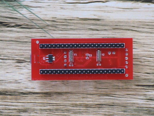
I can’t see anything on the top of the board that looks vaguely like a crystal
It has 2 of those resonator looking devices on the bottom of the board. My guess was that one is the main clock (HSE) and one may be a 32khz RTC
I just checked and APB1 can run at 54Mhz and APB2 can run at 108Mhz, ADC can only run at 14Mhz
The easiest change I can make is just change the PLL down to x 6 and run the board at 72Mhz and all the prescalers should be fine, but I recall testing at that speed when I first started experimenting and I don’t think it made any difference to my issues
But its worth revisiting and confirming.
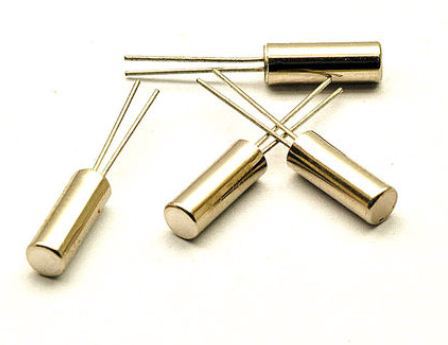
Is it the Y2 crystal ? But on the picture it seems to be 8.000 written on it ?
Is your written 12.000 ?
It is really rare that those crystals are used for high frequencies.
The other doesn’t have any markings.
So I put my scope on Y2 and one side of it is giving me a 200mV 12Mhz sine wave.
Putting the scope on the other side of it, kills the oscillator (I’m not surprised really).
So they are using these cheap crystals / resonators for 12Mhz
I still don’t think that its the issue, but I agree the larger rectangular Xtals are more commonly used at these frequencies
I guess I could change the PLL settings and try a 16Mhz AVR crystal instead.
That was months ago and I dont remember what each function did, but perhaps you see something you are missing:
// rcc_set_prescaler(RCC_PRESCALER_AHB, RCC_AHB_SYSCLK_DIV_1);
rcc_turn_on_clk(RCC_CLK_HSE);
while (!rcc_is_clk_ready(RCC_CLK_HSE))
//board_setup_clock_prescalers();
//rcc_configure_pll(&wirish::priv::w_board_pll_cfg);
rcc_turn_on_clk(RCC_CLK_PLL);
while(!rcc_is_clk_ready(RCC_CLK_PLL)) ;
rcc_switch_sysclk(RCC_CLKSRC_PLL);
The few commented lines were not needed in my case, because the clock prescaler, pll, etc were all still set from running before going to sleep, but the PLL not enabled. So I realised I didn’t need to set again those values, but they worked when included I believe. I am almost sure that is all copied literally from libmaple, but perhaps I added or removed a function call that may help you.
BTW. Did you check how much flash you really have available in these devices?
If you read with stlink up to 128KB, then it has that much flash. When you try to read past an actually valid address, it should give you an error message and stop.
I tried reading past 128k and it just keeps reading.
I tried the same thing on the STM32 and it seems to change the read amount value to 0x20000 i.e 128k
STLink won’t let me write to any address above 64k on either STM32F103C8 of GD32F103C8
I think I’d need to run a test sketch to determine how much flash is really in these devices.
Do you have a test sketch that does this ?
I tried putting in some delays for the HSE stuff (I havent tried Victors code yet), and it doesnt make any difference
I tried dropping the PLL multiplier down to 6 x (12Mhz) so that the board now runs at the same speed as a STM32, and I still get the same error.
Its all a bit flakey.
If I upload using USB to Serial and the hardware bootloader and immediatly execute from 0x800000 it seems to crash.
If I upload the bootloader using STLink, which has the option to reset after upload, it works OK
And it seems to now work OK when I do a power reset.
It doesnt seem to make any difference what speed I select, is 72Mhz and a 1.5 divider for USB works as does 120Mhz with a 2.5 divider. I can see its running at 120Mhz as the led flashes a lot faster at 120Mhz ( also tried 96Mhz and that works OK as well)
I ran DFU-util -l when its running at 120Mhz and I can see all the expected DFU device ALT ID’s, and I know I can upload from within the IDE, but it then crashes in the code ![]()
So I think I’m going to have to fire up GDB and see whats going on, but the problem is that GDB will not understand whats happening after the code jumps to the sketch address, but I guess at that point I need to somehow need to debug a sketch using GDB to see where its crashing
I tried reading past 128k and it just keeps reading.
I tried the same thing on the STM32 and it seems to change the read amount value to 0x20000 i.e 128k
STLink won’t let me write to any address above 64k on either STM32F103C8 of GD32F103C8
I think I’d need to run a test sketch to determine how much flash is really in these devices.
Do you have a test sketch that does this ?
Its not the one in the metal can, but its the firmware that makes the difference and perhaps I’m running an old version of the STLink utility exe
STM32 ST-LINK Utility.exe v3.5.0
STLinkUSB Driver.dll 4.3.3.0
STLINK CLI v 2.1.0
I’ll update the SW in my dongle. But I’m always a bit cautious about doing this in case I “brick” it, but I can always reflash it using usb to serial etc if I need to .
Edit. I seem to have the latest FW already
V2.J23.S4
BTW.
With the STM32 I can only read to 128k on the C8. With the GD32 it just keeps reading.
I put in some really really big sizes (in excess of 1Mb) but it still keeps reading !
So unless they have bunged in some incredibly large flash (as they are a memory manufacturer) then the STLink is not operating the same as on STM32’s
I’ll need to run some sort of Flash test sketch
Does anyone have one ?
Unfortunately, it looks like these GD32F103C8’s are actually only 64k, not 128k like the STM32F103C8 ![]()
It may just be something that is burnt into the hardware, but I can’t seem to use STLink to write above 64k, but I can do it if I upload a 128k file to my Red Pill.
Its a shame really, but I guess this was just a undocumented feature on the STM32F103C8 that we could not rely on, and STM themselves may change in the future
OK. Silly mistake.
I had taken the copy of the STM32 core just after I had applied the PIN MAP in Flash, but before I had updated the Generic STM32F103C variant.
And strangely, this miss match appears to cause GPIO to be unavailable during the stages of initialization when the USB D+ is reset using GPIO.
But, strangely in the sketch GPIO appeared to be available as I could toggle PC13 and flash the LED on the board.
Anyway, Its taken ages to figure out what was going wrong, and in the mean time I’ve done loads of tidy up’s in the code to correctly setup the USB prescaler (which is not present in the STM32 – because there isnt an option to run the board at 48 Mhz – but I now know how to add an option)
BTW. In the end I had to use GDB to debug what was going on, as the code seemed to be calling a function called __error which looks like its a system error trapping function.
(I’m sure Rick could tell us more)
Note(s)
I have put in CPU clock selection, via a menu, with options of 120Mhz, 96Mhz and 48Mhz. I’ve not included 108Mhz as USB is not supported at that speed (even though its the maximum quoted speed).
The bootlloader clock speed seems to need to match the chosen speed for the sketch, so if uploading using the bootloader you need to select 120Mhz.
I suspect this can be fixed, but not tonight. ![]()
The issue with overclocking the STM32 is supposedly the usb prescaler only uses 1 bit and can only divide by 1 and 1.5 x
It uses bit 22 of the rcc config reg, but bit 23 is documented as reserved.
however on the gd32 bits 22 and 23 are used for the usb divider.
So it makes me wonder if bit 23 on the stm32 is really reserved or whether if has an effect, i.e gives the 2 extra prescaler ratios , of 2 and 2.5 x
its probably worth investigating
I wonder why GPIO was working that way, but I can only guess there are some more subtle differences between the STM and the GD. Or perhaps an STM would fail the same way without completing the changes in boards.cpp?
I was reading the other day about the USB port in the F2 and F4 devices. They use 4 bits for pre-escaler, and the usb peripheal itself is different, but someone had been testing overclocking an F2 or F4, I dont remember the model, and he used multipliers that resulted in some cases in 42Mhz for the USB, and still worked.
I wonder if the F1 usb may still work if we get close to 48Mhz without being exact.
The GD USB may also work similar to the STM but not be exactly the same, so even if the F1 can not take anything not exactly 48Mhz, perhaps the GD does. Now that you have USB working, may be worth trying 108Mhz again.
The issue was not a difference in the GPIO, it was my mistake.
When i merged your PIN MAP in flash code, only the Maple mini had the changes to the PIN_MAP array in board.cpp to have pointers to structs.
So when I copied the STM32F1 core to make the GD32 core it didnt have the change in board.cpp to PIN MAP
Strangely when i run normal sketches by uploading using a USB to Serial adaptor, everything worked fine.
But STLink upload crashed as did the bootloader upload.
In the end, I had to use GDB to track down that the crash was when setting PA12 to force USB enumeration, at which point I realised that although I has sub-sequentially updated the STM32F103C board.cpp PIN MAP, I had not copied that change to the GD32 board.cpp
As soon as I updated PIN MAP to use pointers to device structures it stopped crashing.
Re:PLL config Bit 23.
Its going to be easiest to test this by modifying the GD32 bootloader, and change the PLL multiplier to 12 x, as this would give a master clock freq of 96mhz on the STM32s 8 Mhz crystal, and I could also select the 2 x prescaler option, if it exists in bit 23 of the STM32.
Hopefully the STM32 can be overclocked by 30% without having to mess around the the peripheral prescalers as well.
Re: USB at 43.5 Mhz. I suppose its worth a try.
I’m nit sure which is more reliable… Overclocking to 120MHz and having the correct USB. freq, or running the device within spec at 108MHz and using a non standard USB frequency.
I got up early and have tested this.. And I’m afraid, as far as I can tell, Bit 23 has no effect on the STM32.
i.e I reconfigured the GD32 bootloader to run at PLL 9 x multiplier i.e so the STM32 8Mhz crystal gives 72Mhz, and set the USB prescaler value to 0x00 i.e 1.5 and the bootloader worked.
I then tried changing the USB prescaler to 0x02 and this made no difference on my Red Pill
I know my code is working on the GD32, and that Bit 23 definitely does change the USB prescaler.
As a matter of interest, I tried running the Red Pill on PLL of 10 x i,e 80Mhz using the same 1.5 x USB prescaler, but my PC didnt recognise the USB device, so 53.333 Mhz is too fast for USB .
So I also tried changing the PLL to 8 x (i.e 64Mhz, and use the 1.5 prescaler to give 42.6666Mhz ) but this doesnt work on Windows either.
If I drop the PLL right down to 6 x (i.e 48Mhz) and change the prescaler to 0x01 i.e divide by 1, then USB starts working again.
So.
On both counts it looks like, on the STM32, the only possible speeds that can be used, and still run USB are 72Mhz and 48Mhz as bit 23 doesn’t appear to do anything.
It terms of overclocking. I’m pretty sure this has been done before, but I tried changing the PLL multiplier up to 16 x (128Mhz) and my Red Pill is happily flashing its LED in the bootloader (very quickly), so it looks like it can be overclocked as far as the PLL will allow, but you loose USB.
I think there is some code that that was on the Leaflabs forum which would allow a sketch to switch the PLL and to overclock, so it may be worth seeing if USB freaks out, if you overclocked for a while.
But generally, I don’t think its going to be much use, and the GD32 does look like its going to be a faster F103 than the STM32
But… It does look like the F103C8 only has 64k Flash ![]() (But I’d like to do more testing to confirm this)
(But I’d like to do more testing to confirm this)
I’ve one this now, and neither divider of 2.0 or 2.5 works when the PLL is set to x 12 (giving 108Mhz)
Personally, I’m happy to run my GD32’s at 120Mhz, but I guess I could add a bootloader target for 96Mhz (as this works as well, and is within spec)
I think while this is a niche product, most people would rather have as much speed as possible.
Note. At the moment although I’ve added speed selection into the GD32 core board.txt menu i.e 72, 96 or 120Mhz, when using the 120Mhz bootloader, it looks like only the 120Mhz speed option works.
i.e the Sketch speed needs to match the bootloader speed.
I suspect this is because there is a minor problem with the rcc startup code where the the core presumes doesnt fully reset the PLL values.
Actually, I had some issues changing the USB prescaler in the GD32 core, and in the end, found that I had to add the USB prescaler code into the function that sets all the other prescalers, as if I did it later, it seemed to get overwritten – but that could be a red herring, as I’d been working on this problem for quite a few hours last night and things stop making sense after a while.
Anyway. The PLL control etc is greatly enhanced on the GD32 core and even the timings like millis() and delay() now work fine in all the selectable speeds.
Note. Delay never seems totally accurate, so the GD32 stuff is about as accurate as the STM32.
Interestingly, I also see how the millis() works, as its called on by the __systtick callback and is like a timer in that there is a reload value equivalent to the clock frequency e.g. 72000000 – 1, such that the systick function gets called once every millisecond.
Interestingly, systick also has a user callback hook, that is used by the RTOS libs .
However I’m not sure how nanos() works.
Edit.
One more thing.
The hardware on these GD32 board doesnt have a pull up on USB DP (D+), so I had to add a 4.7k resistor (I know sometimes a 1.5k is used as well on some boards)
Anyway, I was hoping to avoid having to add any additional hardware.
However I have tried using the GPIO to drive DP (D+) to 3.3V, and this doesn’t seem to work ![]()
I’d need to read the USB spec, but I presume that DP needs to be pulled above 3.3V to signal to the USB host
Interestingly, systick also has a user callback hook, that is used by the RTOS libs .
…
The hardware on these GD32 board doesnt have a pull up on USB DP (D+), so I had to add a 4.7k resistor (I know sometimes a 1.5k is used as well on some boards)
Anyway, I was hoping to avoid having to add any additional hardware.
However I have tried using the GPIO to drive DP (D+) to 3.3V, and this doesn’t seem to work ![]()
I’d need to read the USB spec, but I presume that DP needs to be pulled above 3.3V to signal to the USB host
Thanks for the info on systick()
Initially I wondered why it had the option to call a user defined callback each time, as I thought it was just wasting CPU time (albeit only once a millisecond), but I then noticed the RTOS stuff uses it, which makes sense.
OK about the 1.5k resistor. I’ll change the resistor I’ve soldered to my board.
I’ve no idea why these GD32 boards don’t have a pullup. USB seems useless without it, and they have connected the USB to the STM32 with 22 ohm resistors and have added static protection as well.
I’ll need to buy a pack of 10 (or more) 1.5k’s from the local electronics shop and mod all my boards, so that USB works on all of them !
See https://www.youtube.com/channel/UCZkTQA … Naj6YdImIA
I’ll cross post about the last video, as I’d like someone to take a look at the Dhrystone tests, which you can see running on the video, as the GD32 seems to have a better Dhrystone speed even at 72Mhz, than the STM32.
Perhaps this is caused by faster access to the Flash or the RAM. I know the Flash architecture is definitely different as they are quoting millions of write cycles, to perhaps this also effects read performance
Do you know where the wait states are configured? Ont the device, I’ve only changed the main PLL and the USB prescaler value, and the systick reload value.
Edit.
I think I found it
#define FLASH_SAFE_WAIT_STATES FLASH_WAIT_STATE_2
Do you know where the wait states are configured? Ont the device, I’ve only changed the main PLL and the USB prescaler value, and the systick reload value.
Edit.
I think I found it
#define FLASH_SAFE_WAIT_STATES FLASH_WAIT_STATE_2
I’d need to try changing it on a STM32, it could be that the register that set this value is either not supported in the GD32, or ignored or perhaps the code doesnt do what we think it does in the core
I better change it to 5 wait states in the stm32 core and see if it makes any difference to the Dhrystone test, but it could be the test is not very dependent on this
There is a separate reg to enable wait states, that I don’t think the STM32 has, which is probably why changing the FLASH_ACR reg is having no effect on the GD32
The 21ic website is furthermore linked to from the Gigadevices site as a “GD32 MCU subsite” so there does seem to be some manufacturer’s tie in to 21ic
21ic does seem to be the main site with stuff about GigaDevices, I suspect they are linked somehow.
I’ve looked on GD’s mini site for their MCU’s but I didnt find a lot there apart from downloading the programming manual for the device (I think I posted a link a to the doc earlier in this thread)
There is supposed to be a different Flash loader exe, but the links to it seem to be dead, but STMs own StLink and Flash uploader seem to work fine.
Re: The HSE stuff.
I don’t think the libmaple core or the bootloader implements the HSE timeout, i.e timeout is infinite, so I could change it to use their code, which seems to do a hard reset if HSE startup times out.
But I’ve never seen this happen, so I’m not sure its worthwhile
I should probably look at the flash programming stuff, because there is an additional test that needs to be run to confirm that after the flash is erased that its ready. But the docs also seem to indicate, just putting 2 nops in the code to delay after the original code thinks the flash is available, is enough to fix it – and in our code, I’m sure its not been an issue, because it will go off any do other stuff after a page of flash has been erased, so its not going to be attempting to write to the newly erased flash within 2 clock cycles of erase being complete.
I noticed some chinglish about Timer Capture Reset being different, but I don’t think the core of the bootloader uses this.
I think there is also a migration doc (cant find it now) from STM32 to GD32, but it didnt seem to have all the changes in it ![]()
That will make things easier than using TaoBao and YoyBuy, which caused me a lot of problems and I ended up with 2 x as many boards as I really wanted ![]()
That will make things easier than using TaoBao and YoyBuy, which caused me a lot of problems and I ended up with 2 x as many boards as I really wanted ![]()
The boards are about $2.50 on Taobao, but when you add shipping an processing, I think the price is at least $5 and probably much more.
The vendor may get more sales if they put “For Arduino” in their details, and also they could reference my repo, as I know have GD32F103 as an option.
Note. The bootloader and USB will not work on this board unless you solder a 1.5k resistor between PA12 and Vdd, as there is a fault in the hardware design (i.e the resistor is missing from the design)
I think the seller update with description.
https://www.openimpulse.com/blog/produc … cortex-m3/
The board you linked to is a STM32, and its a terrible board. I have one and its virtually useless, I’m not sure why but it seems to have problems starting up, I think its an oscillator hardware problem.


