say even if we can do 18 msps x 8 bits it wouldn’t be able to ‘squeeze’ through the 10 mbps usb full speed port
then i think in terms of the bigger SOCs like the ve and ze series and we can patch e.g a 1 MB sram chip via fsmc
that would help with doing a daq (datat aquisition) e.g. oscilloscope, but it would chase up the overall price given the larger soc, sram etc
[arpruss – Sat May 26, 2018 2:09 am] –
I think I misunderstood how 18MS/s is to be achieved. Looking at the reference manual, it looks like one can get 9 MS/s in single mode if one reduces resolution to 6 bits. Presumably, in dual mode that yields the advertised 18 MS/s. At a more reasonable 8 bit resolution, one should be able to use dual interleaved mode to get 14 MS/s, which is still pretty good.
That’s my understanding. It might be possible to have two sets of dual interleaved samples with one set offset from the other but I decided its better to have two slower channels rather than one fast one.
[ag123 – Sat May 26, 2018 7:36 am] –
i’ve been looking at the f3 as the ICs are rather attractively priced, and the most attractive feature is the fast adc, the main issue is the normal usb port is a full speed port 10mbps max (often lesser due to overheads, multiplexing etc)say even if we can do 18 msps x 8 bits it wouldn’t be able to ‘squeeze’ through the 10 mbps usb full speed port
then i think in terms of the bigger SOCs like the ve and ze series and we can patch e.g a 1 MB sram chip via fsmc
that would help with doing a daq (datat aquisition) e.g. oscilloscope, but it would chase up the overall price given the larger soc, sram etc
I don’t think that’s that much of a problem. Relatively early DSO scopes like the Tektronix TDS210 could only do a few thousand samples per channel which can be achieved with the CB and CC chips. You don’t have to sample at the maximum rate, you can drive the ADC by a timer to get pretty much any sample rate you want, and triggering allows you to capture either side of the point you want to look at. Time to transfer data to a PC isn’t so much of an issue then – assuming you’re not driving an small TFT display directly from the MCU.
[dave j – Sat May 26, 2018 11:50 am] – you can drive the ADC by a timer to get pretty much any sample rate you want, and triggering allows you to capture either side of the point you want to look at.
I was thinking of running an acquisition in circular mode, with an analog watchdog interrupt for triggering. Once the trigger interrupt happens, I’ll get the approximate location of the trigger point in the buffer with the DMA NDT register. Then continue running the acquisition until the required number of points after the trigger is acquired (by watching the NDT register and disabling the DMA when we reach the right point). Does that sound right?
Can I drive the ADC by a timer in dual interleaved mode, and have both the master and slave ADCs spaced evenly?
[arpruss – Sat May 26, 2018 1:40 pm] –
I was thinking of running an acquisition in circular mode, with an analog watchdog interrupt for triggering. Once the trigger interrupt happens, get the approximate location of the trigger point in the buffer with the DMA NDT register. Continue running the acquisition until the required number of points after the trigger is acquired (by watching the NDT register and disabling the DMA when we reach the right point). Does that sound right?
Largely. I’m using a second timer, driven by the one that drives the ADC, to count the number of samples captured after a trigger occurs and interrupts when I’ve captured enough. One additional thing to consider is making sure you fill the whole sample buffer. If you capture half a buffer of samples after a trigger you need to make sure you fill the other half before you enable the trigger otherwise you risk having invalid data. If you want to capture half a sample buffer after the trigger you can use the DMA half transfer interrupt and only enable the trigger when responding to that.
So the capturing process would be:
- Start capturing with trigger and post trigger counter disabled but with DMA half transfer interrupt enabled.
- In the DMA half transfer interrupt handler, disable the HT interrupt and enable the trigger interrupt.
- In the trigger interrupt handler, grab the DMA NDT register, enable the post trigger counter and disable the trigger interrupt.
- In the post trigger counter interrupt, stop the conversions.
Can I use drive the ADC by a timer in dual interleaved mode, and have both the master and slave ADCs spaced evenly?
It looks like you can with alternate trigger mode but I’m not sure about doing DMA with the common data register in that mode (doing the latter halves the number of DMA requests which might be significant). If that’s not possible, in interleaved mode you can control when the slave ADC samples relative to the master ADC. My thinking is you could use only the master ADC up to it’s maximum rate and if you want to go faster than that switch to dual interleaved mode, reduce the ADC master rate and use the delay before the slave ADC samples to get evenly spaces samples. See figure 101 in the RM0316 manual.
[dave j – Sat May 26, 2018 3:28 pm] – If you capture half a buffer of samples after a trigger you need to make sure you fill the other half before you enable the trigger otherwise you risk having invalid data.
That’s a good point. Thanks!
If you want to capture half a sample buffer after the trigger you can use the DMA half transfer interrupt and only enable the trigger when responding to that.
Do the half and full transfer interrupts work in circular mode?
So the capturing process would be:
- Start capturing with trigger and post trigger counter disabled but with DMA half transfer interrupt enabled.
- In the DMA half transfer interrupt handler, disable the HT interrupt and enable the trigger interrupt.
- In the trigger interrupt handler, grab the DMA NDT register, enable the post trigger counter and disable the trigger interrupt.
- In the post trigger counter interrupt, stop the conversions.
Isn’t it easier just to have a while loop and watch the NDT register instead of using a timer?
By the way, I am planning to use OsciPrime (with a new source driver) for the UI.
[arpruss – Sat May 26, 2018 5:03 pm] –
Do the half and full transfer interrupts work in circular mode?
Yes. The idea of having them both is so you know you can process half the buffer whilst capturing data into the other half.
Isn’t it easier just to have a while loop and watch the NDT register instead of using a timer?
It depends how your software works. My main loop processes an event queue. Various events (button presses, capture complete, etc.) get added to this queue and processed in turn. Not using the CPU to wait for capture complete means it can do other things in the meantime – displaying a triggered indicator on the UI for instance.
By the way, I am planning to use OsciPrime (with a new source driver) for the UI.
I’m building something standalone driving it’s own screen with a rotary encoder and six buttons for user input. This is what my UI currently look like.
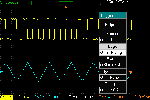
The waveforms are just dummy ones for testing the UI and I’ve still got some bugs to iron out.
[arpruss – Sat May 26, 2018 7:30 pm] –
This is looking really nice!
Thanks. Trying to devise a usable UI with minimal controls has been quite a challenge.
I’m almost at the stage where I really need to decide what to do with my analog input stage. I plan to use the F303’s built in OPAMPs and try and keep things as simple as possible. The problem is -ve voltages, the dev boards only supply +ve ones. For DC coupling it’s not really an issue I can just offset the input like the DPScope SE does. I also want to be able to switch coupling in the UI so a manual switch like the JYETech scopes use won’t do and that means I need to be able to handle -ve voltages in some way. Any suggestions would be welcome.
[Pito – Sat May 26, 2018 11:08 pm] –
You can create -ve (I do not know what voltages/currents you actually need) easily by toggling an output pin (a few kHz) and using 2 diodes (schottky) and 2 capacitors (say 1-10uF ceramics).. For small currents only (say 1-2mA).
It’s to use something like a 4053 to switch between the AC and DC coupled versions of the input signals after the initial voltage divider. I need a -ve voltage for the VEE pin if I want to be able to control inputs that go -ve.
Your idea looks promising – time to do some experimenting.
[dave j – Sat May 26, 2018 11:50 am] –[ag123 – Sat May 26, 2018 7:36 am] –
i’ve been looking at the f3 as the ICs are rather attractively priced, and the most attractive feature is the fast adc, the main issue is the normal usb port is a full speed port 10mbps max (often lesser due to overheads, multiplexing etc)say even if we can do 18 msps x 8 bits it wouldn’t be able to ‘squeeze’ through the 10 mbps usb full speed port
then i think in terms of the bigger SOCs like the ve and ze series and we can patch e.g a 1 MB sram chip via fsmc
that would help with doing a daq (datat aquisition) e.g. oscilloscope, but it would chase up the overall price given the larger soc, sram etcI don’t think that’s that much of a problem. Relatively early DSO scopes like the Tektronix TDS210 could only do a few thousand samples per channel which can be achieved with the CB and CC chips. You don’t have to sample at the maximum rate, you can drive the ADC by a timer to get pretty much any sample rate you want, and triggering allows you to capture either side of the point you want to look at. Time to transfer data to a PC isn’t so much of an issue then – assuming you’re not driving an small TFT display directly from the MCU.
hi dave,
thanks much for the insight indeed TDS210 captures 2500 samples x 2 channel, its samples / sec is much faster though
https://sg.tek.com/document/fact-sheet/ … fact-sheet
that gives me the inspiration to get an f3 which i ignored earlier
at 18msps it would be possible to observe signals in the low mhz ranges e.g. spi etc


