http://www.st.com/content/ccc/resource/ … 031020.pdf
vs RM0008 reference manual for F1*
http://www.st.com/content/ccc/resource/ … 171190.pdf
there a a lot of parts that looked literally ‘identical’, how i hoped pdf viewers can do a ‘diff’ and just tell me what are the differences ![]()
i noted the following as 1 of the difference:
STM32F1 RM0008 p710 25.3.3 Configuring the SPI in master mode
25.3.3 Configuring the SPI in master mode
Procedure
1. Select the BR[2:0] bits to define the serial clock baud rate (see SPI_CR1 register).
2. Select the CPOL and CPHA bits to define one of the four relationships between the data transfer and the serial clock (see Figure 239).
3. Set the DFF bit to define 8- or 16-bit data frame format
4. Configure the LSBFIRST bit in the SPI_CR1 register to define the frame format.
5. If the NSS pin is required in input mode, in hardware mode, connect the NSS pin to a high-level signal during the complete byte transmit sequence. In NSS software mode, set the SSM and SSI bits in the SPI_CR1 register. If the NSS pin is required in output
mode, the SSOE bit only should be set.
6. The MSTR and SPE bits must be set (they remain set only if the NSS pin is connected
to a high-level signal). In this configuration the MOSI pin is a data output and the MISO pin is a data input.
STM32F1 RM0009 p887 28.3.3. Configuring the SPI in master mode
28.3.3. Configuring the SPI in master mode
In the master configuration, the serial clock is generated on the SCK pin.
Procedure
1. Select the BR[2:0] bits to define the serial clock baud rate (see SPI_CR1 register).
2. Select the CPOL and CPHA bits to define one of the four relationships between the data transfer and the serial clock (see Figure 248). This step is not required when the TI mode is selected.
3. Set the DFF bit to define 8- or 16-bit data frame format
4. Configure the LSBFIRST bit in the SPI_CR1 register to define the frame format. This step is not required when the TI mode is selected.
5. If the NSS pin is required in input mode, in hardware mode, connect the NSS pin to a high-level signal during the complete byte transmit sequence. In NSS software mode, set the SSM and SSI bits in the SPI_CR1 register. If the NSS pin is required in output mode, the SSOE bit only should be set. This step is not required when the TI mode is selected.
6. Set the FRF bit in SPI_CR2 to select the TI protocol for serial communications.
7. The MSTR and SPE bits must be set (they remain set only if the NSS pin is connected to a high-level signal).
configuration the MOSI pin is a data output and the MISO pin is a data input.
while this is unlikely to be the only difference what seem rather distinct is this addition of the ‘TI mode’
a timing diagram is given on p887 RM0009 SPI TI protocol in master mode
apparently the ‘TI mode’ seemed to have things like ‘triggering edge’ and ‘sampling edge’ and it seem to start with single NSS high pulse sequence
the other ‘strange’ thing about this P887 RM0009 SPI TI protocol timing diagram is it seem to label MOSI as ‘input’ while MISO as ‘output’ this doesn’t seem to match the notions of how we’d usually do SPI since stm32 is the ‘master’ (seemed more like an error in the diagram)
my thoughts are in step (6) above, we’d need to *switch off* TI mode to get the ‘regular’ SPI we’d expect
in particular if we do use the NSS pin as a custom /CS pin for the SPI devices (i always do that so as not to ‘waste’) pins ![]()
but then the default for SPI_CR2 FRF at reset seem to be 0 motorola mode (rather than 1 TI mode)
just 2 cents
stm32 also use the same boundary addresses and register addresses for SPI1 and SPI2, SPI3
0x4001 3000 – 0x4001 33FF SPI1
0x4000 3800 – 0x4000 3BFF SPI2/I2S
0x4000 3C00 – 0x4000 3FFF SPI3 / I2S3
as after all the F4 runs at 168 mhz while an F1 runs at 72 mhz, lots of things to hunt down to figure out differences esp if things don’t work
the TI mode it seemed is that additional use of the NSS pin which based on the RM is default off and motorola mode is used instead
another thing which we may need to check may be to see if a particular peripheral bus is clocked.
found a web that seemed useful on the topic of clocks
https://stm32f4-discovery.net/2015/01/p … x-devices/
settings seem to match that used on steves F4 black branch, the PLL multipliers seemed similar
https://github.com/stevstrong/Arduino_S … cF4.c#L431
void SetupClock168MHz() {

...

// save bus clock values

rcc_dev_clk_speed_table[RCC_AHB1] = (SystemCoreClock/1);

rcc_dev_clk_speed_table[RCC_APB2] = (SystemCoreClock/2);

rcc_dev_clk_speed_table[RCC_APB1] = (SystemCoreClock/4);
Now need to determine which of my changes made it.
More to come.
Now need to determine which of my changes made it.
More to come.
Type any character to start

FreeStack: 117044

Type is FAT32

Card size: 15.93 GB (GB = 1E9 bytes)
Manufacturer ID: 0X3

OEM ID: SD

Product: SL16G

Version: 8.0

Serial number: 0X72F2CA43

Manufacturing date: 8/2015
File size 5 MB

Buffer size 512 bytes

Starting write test, please wait.
write speed and latency

speed,max,min,avg

KB/Sec,usec,usec,usec

375.32,122150,759,1363

387.66,18954,1021,1319
Starting read test, please wait.
read speed and latency

speed,max,min,avg

KB/Sec,usec,usec,usec

945.83,1574,529,540

946.01,1071,529,540
Done
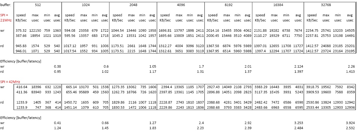
writing speed seem to have reached sd native limiting speed, for read speed, my thoughts are that if a bigger buffer is used e.g. 1k it may narrow the difference so much that DMA would not make too much difference
- stm32_sd_performance.jpg (162.89 KiB) Viewed 921 times
But even with 8k buffer it gives a nice speed.
SdBench with F1 must give you ~3.5MB/sec rd/wr @36MHz SPI clock and SdFatEX with 512bytes large buffer and DMA on..
I don’t see any way how to increase 10 times the rd/wr speed…
Can you hint to any solution?
Again, the above results are real..
Oh, and send me a similar card you are using ![]()
Btw, which color is your Sammy card? red or yellow/orange?
The cards I have used are:
1. Samsung EVO 8GB, CL10 UHS-I (white/orange) – works 21, 36, 42MHz
2. Sandisk Ultra 16GB, CL10 (red/grey) – works 21, 36MHz
If you do not get such results (plus minus 0.2MB/sec) then it is something wrong with your setup/settings/SPI_DMA driver..
The same results I get with Daniel’s core, and with libmaple.
With SdFatEX use 512bytes large buffer.
You can also send me BIN files for blue pill and/or maple mini and/or black F4 + indicate the used SPI and CS pins for each board in part.
You have to get something like:
File size 5 MB

Buffer size 512 bytes

Starting write test, please wait.
write speed and latency
speed,max,min,avg
KB/Sec,usec,usec,usec
3533.34,25083,136,143
3594.74,15522,136,141
Starting read test, please wait.
read speed and latency
speed,max,min,avg
KB/Sec,usec,usec,usec
3257.12,1548,155,156
3258.89,1359,155,156
Done
Type any character to start
FYI – the min Latency is the time you need to transfer 512bytes to the Sdcard. From above results:
136us/512/8 = 33.2ns -> 30MHz
207us/512/8 = 50.5ns -> 19.8MHz
I also observed that the F1 bench BIN is 38kB large, while the F4 BIN is 28kB large (smaller than the F1 bin). Is this really how it should be?
EDIT
Flashing the MM over DFU:
>maple_upload.bat COM3 2 1EAF:0003 sdbench_f1.bin

maple_loader v0.1

Resetting to bootloader via DTR pulse

Reset via USB Serial Failed! Did you select the right serial port?

Assuming the board is in perpetual bootloader mode and continuing to attempt dfu programming...
Searching for DFU device [1EAF:0003]...
Found it!
Opening USB Device 0x1eaf:0x0003...
Found Runtime: [0x1eaf:0x0003] devnum=1, cfg=0, intf=0, alt=2, name="STM32duino bootloader v1.0 Upload to Flash 0x8002000"
Setting Configuration 1...
Claiming USB DFU Interface...
Setting Alternate Setting ...
Determining device status: state = dfuIDLE, status = 0
dfuIDLE, continuing
Transfer Size = 0x0400
bytes_per_hash=761
Starting download: [##################################################] finished!
state(8) = dfuMANIFEST-WAIT-RESET, status(0) = No error condition is present
error resetting after download: usb_reset: could not reset device, win error: The system cannot find the file specified.
Done!
Resetting USB to switch back to runtime mode
I also observed that the F1 bench BIN is 38kB large, while the F4 BIN is 28kB large (smaller than the F1 bin). Is this really how it should be?
I recompiled it again with
File: SDBench.bin
CRC-32: eb38f0d4
MD4: 4d43be8aa4f0f8ad05d059f6e981fad2
MD5: 5aec1c4acfb959f8c81e480981836786
SHA-1: e7b93691e776f2df4012b1713380df174948b589
- SDBench.rar
- (18.25 KiB) Downloaded 17 times
nothing on serial 1…
Sh…t, it was a loose wire, sorry.
Which one is the CS pin? PB6?
FreeStack: 128032

Can't access SD card. Do not reformat.

No card, wrong chip select pin, or SPI problem?

SD errorCode: 0X20,0XFF
On PB6, as said, i get the clock signal..
Where is PB4 on the black board?
- SDBench_F1.rar
- (17.86 KiB) Downloaded 15 times
File size 5 MB

Buffer size 512 bytes

Starting write test, please wait.
write speed and latency

speed,max,min,avg

KB/Sec,usec,usec,usec

2397.93,19155,207,212

2399.08,16532,207,212

2412.97,15940,207,211
Starting read test, please wait.
read speed and latency

speed,max,min,avg

KB/Sec,usec,usec,usec

2446.03,1590,208,208

2447.22,972,208,208

2447.22,972,208,208
Done
I realized that it is not enough to set in SdFatConfig.h,
#define ENABLE_EXTENDED_TRANSFER_CLASS 1Bench for Black F4 @ 168MHz, SPI1 @ 21MHZ, with DMA, SdFatEX, Sandisk Ultra 16GB, CL10 (red/grey):
File size 5 MB

Buffer size 512 bytes

Starting write test, please wait.
write speed and latency
speed,max,min,avg
KB/Sec,usec,usec,usec
2438.87,13975,204,208
2446.03,14013,204,208
Starting read test, please wait.
read speed and latency
speed,max,min,avg
KB/Sec,usec,usec,usec
2499.84,1448,203,204
2501.09,909,203,204
File size 5 MB

Buffer size 512 bytes

Starting write test, please wait.
write speed and latency

speed,max,min,avg

KB/Sec,usec,usec,usec

4393.39,7474,112,114

4328.73,10052,112,116

4378.00,7742,112,115
Starting read test, please wait.
read speed and latency

speed,max,min,avg

KB/Sec,usec,usec,usec

3887.78,975,129,130

3887.78,836,129,130

3890.80,835,129,130
Your F1 results look very close to be proportional to my ones, which were done at 36MHz:
44MHz/36MHz = 1.222
WR speed: (my result) 3.7 * 1.22 = 4.5, your result is ~4.4
RD speeed: (my result) 3.38 * 1.22 = 4.1, your result is ~3.9
Similar proportionality is achieved for F4 @ 42MHz WR speed: ~4.6.
I find it interesting that the F4 RD result is not proportional anymore, ~4.8 being ~20% higher than F1 performs using the same card, although the SPI code for F4 is very similar to F1 code.
I only can think that the difference is made by the CPU clock.
So it seems to be a general difference/issue somewhere.
