im using a Maple mini clone (stm32f103) with the Arduino ide where the BOOT1 pin is wired through a 100k resistor to PB2.
For my project i need the whole 16 bits of Port B to which i am writing 16 Bit data by a DMA channel.
Is it possible to remap the output of PB2 to another gpis pin, e.g. PA15?
You may want to use a different board, such as the bluepill, or some other of the generic boards if you really need to use that pin.
In this case you should simply shorten the 100k resistor and connect whatever you want to middle pin of BOOT1 jumper block.
I dont think you need to do anything about it.
You could of course just cut the track with a sharp knife. or unsolder the resistor
I dont think you need to do anything about it.
You could of course just cut the track with a sharp knife. or unsolder the resistor
No worries.
These boards are as cheap as chips, so the OP may as well get another one, as long as they are willing to wait for it to arrive
No worries.
These boards are as cheap as chips, so the OP may as well get another one, as long as they are willing to wait for it to arrive
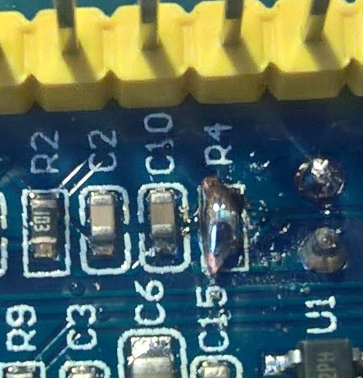
Thanks for the reply. I have now shorted R4 and wired the TFT as in the photos. However, when I try to compile the graphicstest example from your library, I get these errors
C:\Users\Steve\Documents\Arduino\libraries\Adafruit_TFTLCD_8bit_STM32-master\Adafruit_TFTLCD_8bit_STM32.cpp:489:21: error: ‘readReg32’ was not declared in this scope
and
C:\Users\Steve\Documents\Arduino\libraries\Adafruit_TFTLCD_8bit_STM32-master\Adafruit_TFTLCD_8bit_STM32.cpp:499:31: error: ‘readReg32’ was not declared in this scope
Any thoughts?
Steve.
- short.jpg (168.95 KiB) Viewed 1422 times
https://github.com/stevstrong/Adafruit_ … M32.h#L153
You could simply insert in line 153 of the header file following line:
extern uint32_t readReg32(uint8_t r);Thanks for the update, I can now build and upload the code however, th screen remains white. I have several different screens, all of which work on the UNO/Mega2560 using mcufriend_kbv. I had hoped one would work with this driver. The screen I’d really lke to get working is an MCUFRIEND 3.95″ SPI+8 bit withe ILI9488.
Now, I noticed in the header file you ammended that the TFT_RST was on PB8 (see below) when I was sure I had read it should be on PA4 however, I tried both with no success. It’s getting verry frustrating not having a screen working with the ‘pill’ when they work with the Arduinos and I really want to be moving up to STM32duino’s instead.
#define TFT_DATA       GPIOB

// Port data bits D0..D7:

// enable only one from below lines corresponding to your HW setup:

#define TFT_DATA_NIBBLE	0 // take the lower 8 bits: 0..7

//#define TFT_DATA_NIBBLE	8 // take the higher 8 bits: 8..15
//Control pins |RD |WR |RS |CS |RST|
#define TFT_CNTRL GPIOA
#define TFT_RD PA0
#define TFT_WR PA1
#define TFT_RS PA2
#define TFT_CS PA3
#define TFT_RST PB8 //PB0
Just adapt the pins you have wired, using PXY notation (e.g. PA3).
I was using it as well to debug my setup, and could successful correct my errors based on that.
You could maybe post here the log output.
And yes, those changes should suffice.
- WP_20170223_20_17_07_Pro.jpg (213.93 KiB) Viewed 575 times
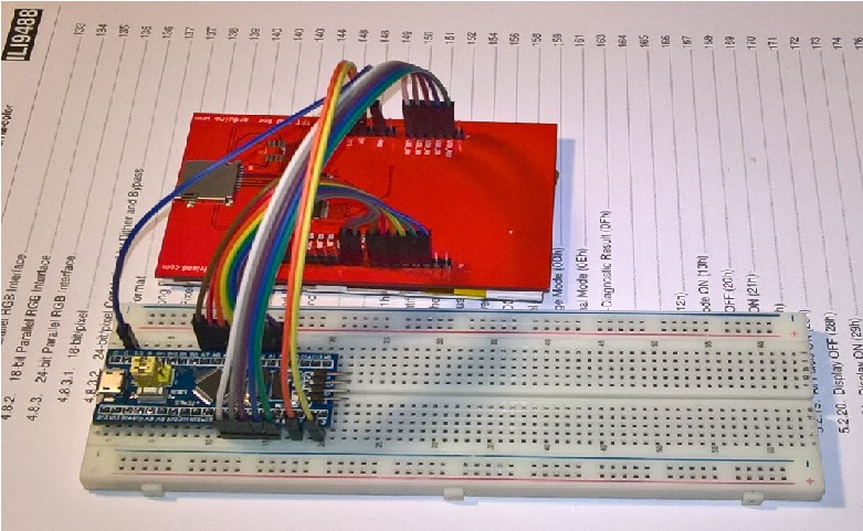
I also connected the shield to a CZ miniSTM32F103VEK board using the same pins, Data on A0-A7 & CTRL on B3-B7.
I got the exact same result.
Steve F
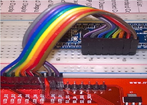
Be aware, that the data pins on the display board are not consecutively numbered. D0 and D1 are twisted and are placed on the other connector than D2..D7. At least I think so, because it is the case on my 2.4 inch TFT module.
Can you post here a picture of the back side of the board? Is it like this one?
- wires.jpg (184.48 KiB) Viewed 562 times
Aaarghhhh!
I remember, there are some pins (including PB4) which only work if some define is active, dependent on some upload method (it is related to debug port, if you search the forum for “PB4” you will have something to read about).
I think the solution is to remove “-DCONFIG_MAPLE_MINI_NO_DISABLE_DEBUG=1” from boards.txt line 193.
As an alternative, I would suggest to use any other (PB_0/1/9/10/11 ?) pin instead PB4 (which is connected to RD control signal – critical for reading!).
Write a short test sketch just to toggle each of the used pins (both data and control) with an external LED connected (or check with a scope).
It was so much easier to move all the pins across to PB5..PB9 and redefine in the sketch and you, I get sensible results
No to edit the hearer file and try the graphics test …. I may be some time
Read Registers on STM32duino

controllers either read as single 16-bit

e.g. the ID is at readReg(0)

or as a sequence of 8-bit values

in special locations (first is dummy)
reg(0x0000) 00 00 ID: ILI9320, ILI9325, ILI9335, ...
reg(0x0004) 00 54 80 66 Manufacturer ID
reg(0x0009) 00 00 61 00 00 Status Register
reg(0x000A) 00 08 Get Powsr Mode
reg(0x000C) 00 06 Get Pixel Format
reg(0x0061) 00 00 RDID1 HX8347-G
reg(0x0062) 00 00 RDID2 HX8347-G
reg(0x0063) 00 00 RDID3 HX8347-G
reg(0x0064) 00 00 RDID1 HX8347-A
reg(0x0065) 00 00 RDID2 HX8347-A
reg(0x0066) 00 00 RDID3 HX8347-A
reg(0x0067) 00 00 RDID Himax HX8347-A
reg(0x0070) 00 00 Panel Himax HX8347-A
reg(0x00A1) 00 93 30 93 30 RD_DDB SSD1963
reg(0x00B0) 00 00 RGB Interface Signal Control
reg(0x00B4) 00 02 Inversion Control
reg(0x00B6) 00 02 02 3B 3B Display Control
reg(0x00B7) 00 06 Entry Mode Set
reg(0x00BF) 00 00 00 00 00 00 ILI9481, HX8357-B
reg(0x00C0) 00 0E 0E 0E 0E 0E 0E 0E 0E Panel Control
reg(0x00C8) 00 B0 B0 B0 B0 B0 B0 B0 B0 B0 B0 B0 B0 GAMMA
reg(0x00CC) 00 03 Panel Control
reg(0x00D0) 00 00 00 Power Control
reg(0x00D2) 00 00 00 00 04 NVM Read
reg(0x00D3) 00 00 94 88 ILI9341, ILI9488
reg(0x00DA) 00 54 RDID1
reg(0x00DB) 00 80 RDID2
reg(0x00DC) 00 66 RDID3
reg(0x00E0) 00 00 07 0C 05 13 09 36 AA 46 09 10 0D 1A 1E 0F GAMMA-P
reg(0x00E1) 00 00 20 23 04 10 06 37 56 49 04 0C 0A 33 37 0F GAMMA-N
reg(0x00EF) 00 00 00 00 00 00 ILI9327
reg(0x00F2) 00 58 04 12 02 22 22 FF 0A 90 14 88 Adjust Control 2
reg(0x00F6) 00 00 00 00 Interface Control
It still no workee! It reports the following;
TFT LCD test

TFT size is 240x320

ID: 0
*** Unknown LCD driver chip: 0
I am actually glad if someone has time to add value to the lib.
You could collect info about your display controller in David Prentice’s repo (mcufriends_kbv) and add in to my one, in order to work with original Adafruit functions and GFX lib.
EDIT
You can see here the resulted graphicstest benchmark.
Am going home Wednesday morning and probably won’t get time to do anything more until im back in UK two weeks later as Bev probably has a list of jobs for me!
Steve F.
