STM32F103ZET6 Minimum System Development Board ARM STM32 Cortex-m3 M75
from
http://www.ebay.co.uk/itm/291305557264? … EBIDX%3AIT
i2c scanner(from examples) shows this
Scanning…
I2C device found at address 0x50
I2C device found at address 0x51
I2C device found at address 0x52
I2C device found at address 0x53
done
the device address is known to be 0x50, so is this just bad address decoding or is it really returning 4 devices?
i’m inclined to the former:-)
the data sheet says single address and im trying to write and then read back from a location; mention is made of
a ‘repeated start.
so my code
int data;

#define Trigger PB3
void setup() {
pinMode(Trigger, OUTPUT);
digitalWrite(Trigger, LOW);
Serial.begin(115200);
Wire.begin();
}
void loop() {
digitalWrite(Trigger, HIGH); // ols trigger
Wire.i2c_start();
Wire.i2c_shift_out(0x50); // device address
Wire.i2c_get_ack();
Wire.i2c_shift_out(0x5a); // writing data to this address
Wire.i2c_get_ack();
Wire.i2c_shift_out(0xa5); // write data
Wire.i2c_get_ack();
Wire.i2c_stop();
delay(5);
Wire.i2c_start();
Wire.i2c_shift_out(0x50); // device address
Wire.i2c_get_ack();
Wire.i2c_shift_out(0x5a); // writing data to this address
Wire.i2c_get_ack();
data = Wire.i2c_shift_in(); // write data
Wire.i2c_get_ack();
Wire.i2c_stop();
digitalWrite(Trigger, LOW); //
delay(5);
}
all as expected per circuit diagram. b6/b7 to chip & 4k7’s come as 4k67 to 3v3 pin; i’ll live with 0.64% low
the spi flash is definitely marked as a Winbond 25X40BVN1G
data sheet says
Atmel AT24C08C, 8K Serial EEPROM: Internally organized with 64 pages of 16 bytes each, the 8K requires a 10-bit
data word address for random word addressing.
Acknowledge: All addresses and data words are serially transmitted to and from the EEPROM in eight bit words. The
EEPROM sends a zero to acknowledge that it has received each word. This happens during the ninth clock cycle.
crafty little b’s aren’t they(datasheets that is:-)
i was using pb3 as a trigger for the ols and getting a load of side effect, so switched to pg14
trigger line is now a single pulse!
stephen
all the sda data seems to span the 8 clks and is extended to the first pulse for the next transmission
how do i send a set of 9 clocks as this is what seems to shift it left?
stephen
what i was trying to do was set the location in the chip that i want to read data from.
a complication is that it needs a 10 bit location, 0x00-0x3ff which i interpret as sending 2 bytes;
and i keep seeing a nack after the first.
others are
1. a repeated start?
2. nine clock cycles, i’ve only seen any mention of 9 bits in bit-bang i2c code
stephen
Here are the snippet of code :
void WireEepromWriteByte(uint16_t theMemoryAddress, uint8_t u8Byte)

{

Wire.beginTransmission(EEPROM_ADDRESS);

Wire.write( (theMemoryAddress >> 8) & 0xFF );

Wire.write( (theMemoryAddress >> 0) & 0xFF );

Wire.write(u8Byte);

Wire.endTransmission();

delay(5);

}
uint8_t WireEepromRead(uint16_t theMemoryAddress)
{
uint8_t u8retVal = 0;
Wire.beginTransmission(EEPROM_ADDRESS);
Wire.write( (theMemoryAddress >> 8) & 0xFF );
Wire.write( (theMemoryAddress >> 0) & 0xFF );
Wire.endTransmission();
delay(5);
Wire.requestFrom(EEPROM_ADDRESS, 1);
u8retVal = Wire.read();
return u8retVal ;
}
#include <Wire.h>
#define EEPROM_ADDRESS  0x50

byte data = 0;

#define Trigger PG14
void setup() {

pinMode(Trigger, OUTPUT);

digitalWrite(Trigger, LOW);   // set trigger off)

Wire.begin();

}
void loop()

{

digitalWrite(Trigger, HIGH);   // ols trigger

digitalWrite(Trigger, LOW);   // ols trigger

delayMicroseconds(200);

WireEepromWriteByte(0x55, 0xaa);

data = WireEepromRead(0x55);

}
The datasheet http://www.atmel.com/Images/doc3256.pdf mentioned that the addressing is done with a single byte, higher bits from the address should be ORed with the EEPROM address, so it is NOT 2 bytes addressing.
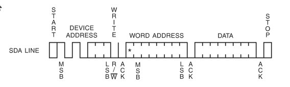
- 24c08.jpg (12.55 KiB) Viewed 1099 times
Figure 8-1. Device Address
Density Access Area Bit 7 Bit 6 Bit 5 Bit 4 Bit 3 Bit 2 Bit 1 Bit 0
8K EEPROM 1 0 1 0 A2 P1 P0 R/W
in fact i’m fairly sure i did a find on p1/p0, that table is the only place they occur
shouldn’t have got out of tech pubs that way
Standard EEPROM Access: The 4K and 8K EEPROM device requires an 8-bit device address word following a start
condition to enable the chip for a read or write operation. The device address word consists of a mandatory “1010” (0xA)
sequence for the first four Most Significant Bits (MSB) as shown in Figure 8-1 on page 11. This is common to all the
EEPROM devices.
The 4K EEPROM only uses the A2 and A1 device address bits with the third bit being a memory page address bit. The
two device address bits must compare to their corresponding hard-wired input pins. The A0 pin is no connect.
The 8K EEPROM only uses the A2 device address bit with the next two bits being for memory page addressing. The A2
address bit must compare to its corresponding hard-wired input pin. The A1 and A0 pins are no connect.
The eighth bit of the device address is the read/write operation select bit. A read operation is initiated if this bit is high and
a write operation is initiated if this bit is low.
thanks
IMHO, its probably work looking at libs that other people have written ( unless you are doing this just to improve your understanding of this chip and of I2C)
I will try to find it again, either on my drives or on the net …
So, @zmemw16, did you got chance to do some real Read/Write into your ?
void WireEepromWriteByte(uint16_t theMemoryAddress, uint8_t u8Byte) {

Wire.beginTransmission( EEPROM_ADDRESS | ( ( theMemoryAddress >> 8 ) & 0x3 ) );

Wire.write( theMemoryAddress  & 0xFF );

Wire.write(u8Byte);

Wire.endTransmission();

delay(5);

}
uint8_t WireEepromRead(uint16_t theMemoryAddress) {

Wire.beginTransmission( EEPROM_ADDRESS | (  ( theMemoryAddress >> 8 ) & 0x3 ) );

Wire.write( theMemoryAddress  & 0xFF );

Wire.endTransmission();

delay(5);

Wire.requestFrom( (EEPROM_ADDRESS | (theMemoryAddress >> 8) & 0x3), 1);

return Wire.read();

}
stephen
I will try to find it again, either on my drives or on the net …
Thanks
I will try to test that library at the weekend. I have multiple f103vet board, because of a screw up in eBay, and also 1 x f103zet, all of which have external EEPROMS
i need to look at the diagrams again.
i also have a couple or more of 103 vet & zet boards, one or more have lcd connections.
there is a serious lot of variation in the lcd connections. 32/36/37/40 pins, 9 or 16 data lines, spi, /rd, /wr, touch etc etc
my next question is how do you find out how to drive one? i had a look at CubeMX and it appears to be down to
the vagaries of the wind as to how the FMSC is configured?
but i suspect that that’s another thread….
stephen
SPI and I2C work fine in the Maple core.
Various displays have been ported, but they are mainly the I2C and SPI interface variety, however I think a few people were investigating porting some of the libs for the parallel connection displays
I have one of those 3.2in touch + LCD + SD screens, that has a 16 bit data path to the LCD, but I just don’t have time even to wire the thing up, let alone start looking at the libraries ;-(
who went the computers, software and hardware interfaces route – i seem to be collecting assorted electronics.
keep me from too much tv couch in the long winter evenings:-)
so i have one or two 3.2 & other sizes tft lcd + touch + sd as well
actually i was looking at cubemx as it occurs to me that at some point these ‘enhanced’ boards need to be made usable and how do we in effect reverse engineer the ‘addressing’ of the enhancements.
thoughts from the variation of lcd connectors i’ve got so far,
i’ve got to find some 40 pin ide cables, extra long and with three connectors.
what would really make it easier would be port wide operations, 8 & 16 bits; maybe that already exists?
maybe a way of merging ‘bits’ such that you could read/write 8 or 16 bits hiding the way they might be split up
pa0-pa3, pb4-pb7, pc0, pc3, pd4-pd9 sort of thing.
my excuse is it’s 0415
stephen
You’d need to write to the output data register, but its really easy, I think its something like
GPIOA->dev->odr = 0x1234;


