I continue to work on putting the pieces together for my port of YMFC-32 STM32F103 based flight controller. The application reads pilot commands in from a PPM stream, with input pulse widths to be measured using on of the STM32 TIM channels. The application also reads a combined accelerometer/gyro (MPU-6050) over I2C. I’ve chosen I2C1 with alternate function inputs (SDA on PB9 and SCL on PB8). The default for I2C1 are PB7 (SDA) and PB6 (SCL).
The PPM stream comes from a 5V powered receiver, the voltage levels from the Rx outputs are not specified so I have chosen to use TIM4 as it is the only F103RB TIM with 5V tolerant inputs. I elected to use TIM_CH1 to measure the input stream, which turns out to be PB6. I’ve attached a picture of the test setup.
I had previously tested the I2C sensor wiring using I2C Scanner test sketch. The sketch consistently showed the MPU-6050 found at address 0x68, as expected. I then wired up the PPM generator and that is when the trouble started. With the PPM generator wired in at PB6 and no other changes the I2C Scanner test sketch gave errors and was no longer able to find the MPU-6050 at 0x68 or any other address.

George

Ok you didn’t finish your post
Do you use pull UP resistor on i2c line ?
Studying this function shows that it enables the I2C1 peripheral clock and forces a reset before the GPIO and pin alternate function code is executed. Meanwhile the PPM generator is active on PB6 and the I2C peripheral is getting SCL inputs clocked in before PB8/PB9 are assigned to I2C1.
Shouldn’t GPIO/AF initialization occur before I2C peripheral is activated?
When I modify i2c_custom_init() to do pin initialization first the I2C Scanner, the errors go away and things work as expected.
/**

* @brief  Default init and setup GPIO and I2C peripheral

* @param  obj : pointer to i2c_t structure

* @retval none

*/

void i2c_init(i2c_t *obj)

{

i2c_custom_init(obj, I2C_100KHz, I2C_ADDRESSINGMODE_7BIT, 0x33, 1);

}
/**
* @brief Initialize and setup GPIO and I2C peripheral
* @param obj : pointer to i2c_t structure
* @param timing : one of the i2c_timing_e
* @param addressingMode : I2C_ADDRESSINGMODE_7BIT or I2C_ADDRESSINGMODE_10BIT
* @param ownAddress : device address
* @param master : set to 1 to choose the master mode
* @retval none
*/
void i2c_custom_init(i2c_t *obj, i2c_timing_e timing, uint32_t addressingMode, uint32_t ownAddress, uint8_t master)
{
if(obj == NULL)
return;
GPIO_InitTypeDef GPIO_InitStruct;
GPIO_TypeDef *port;
I2C_HandleTypeDef *handle = &(obj->handle);
// Determine the I2C to use
I2C_TypeDef *i2c_sda = pinmap_peripheral(obj->sda, PinMap_I2C_SDA);
I2C_TypeDef *i2c_scl = pinmap_peripheral(obj->scl, PinMap_I2C_SCL);
//Pins SDA/SCL must not be NP
if(i2c_sda == NP || i2c_scl == NP) {
core_debug("ERROR: at least one I2C pin has no peripheral\n");
return;
}
obj->i2c = pinmap_merge_peripheral(i2c_sda, i2c_scl);
if(obj->i2c == NP) {
core_debug("ERROR: I2C pins mismatch\n");
return;
}
#if defined I2C1_BASE
// Enable I2C1 clock if not done
if (obj->i2c == I2C1) {
__HAL_RCC_I2C1_CLK_ENABLE();
__HAL_RCC_I2C1_FORCE_RESET();
__HAL_RCC_I2C1_RELEASE_RESET();
obj->irq = I2C1_EV_IRQn;
#if !defined(STM32F0xx) && !defined(STM32L0xx)
obj->irqER = I2C1_ER_IRQn;
#endif // !defined(STM32F0xx) && !defined(STM32L0xx)
i2c_handles[0] = handle;
}
#endif // I2C1_BASE
#if defined I2C2_BASE
// Enable I2C2 clock if not done
if (obj->i2c == I2C2) {
__HAL_RCC_I2C2_CLK_ENABLE();
__HAL_RCC_I2C2_FORCE_RESET();
__HAL_RCC_I2C2_RELEASE_RESET();
obj->irq = I2C2_EV_IRQn;
#if !defined(STM32F0xx) && !defined(STM32L0xx)
obj->irqER = I2C2_ER_IRQn;
#endif // !defined(STM32F0xx) && !defined(STM32L0xx)
i2c_handles[1] = handle;
}
#endif // I2C2_BASE
#if defined I2C3_BASE
// Enable I2C3 clock if not done
if (obj->i2c == I2C3) {
__HAL_RCC_I2C3_CLK_ENABLE();
__HAL_RCC_I2C3_FORCE_RESET();
__HAL_RCC_I2C3_RELEASE_RESET();
obj->irq = I2C3_EV_IRQn;
#if !defined(STM32F0xx) && !defined(STM32L0xx)
obj->irqER = I2C3_ER_IRQn;
#endif // !defined(STM32F0xx) && !defined(STM32L0xx)
i2c_handles[2] = handle;
}
#endif // I2C3_BASE
#if defined I2C4_BASE
// Enable I2C4 clock if not done
if (obj->i2c == I2C4) {
__HAL_RCC_I2C4_CLK_ENABLE();
__HAL_RCC_I2C4_FORCE_RESET();
__HAL_RCC_I2C4_RELEASE_RESET();
obj->irq = I2C4_EV_IRQn;
#if !defined(STM32F0xx) && !defined(STM32L0xx)
obj->irqER = I2C4_ER_IRQn;
#endif // !defined(STM32F0xx) && !defined(STM32L0xx)
i2c_handles[3] = handle;
}
#endif // I2C4_BASE
//SCL
port = set_GPIO_Port_Clock(STM_PORT(obj->scl));
GPIO_InitStruct.Pin = STM_GPIO_PIN(obj->scl);
GPIO_InitStruct.Mode = STM_PIN_MODE(pinmap_function(obj->scl,PinMap_I2C_SCL));
GPIO_InitStruct.Speed = GPIO_SPEED_FREQ_HIGH;
GPIO_InitStruct.Pull = STM_PIN_PUPD(pinmap_function(obj->scl,PinMap_I2C_SCL));
#ifdef STM32F1xx
pin_SetF1AFPin(STM_PIN_AFNUM(pinmap_function(obj->scl,PinMap_I2C_SCL)));
#else
GPIO_InitStruct.Alternate = STM_PIN_AFNUM(pinmap_function(obj->scl,PinMap_I2C_SCL));
#endif /* STM32F1xx */
HAL_GPIO_Init(port, &GPIO_InitStruct);
//SDA
port = set_GPIO_Port_Clock(STM_PORT(obj->sda));
GPIO_InitStruct.Pin = STM_GPIO_PIN(obj->sda);
GPIO_InitStruct.Mode = STM_PIN_MODE(pinmap_function(obj->sda,PinMap_I2C_SDA));
GPIO_InitStruct.Speed = GPIO_SPEED_FREQ_HIGH;
GPIO_InitStruct.Pull = STM_PIN_PUPD(pinmap_function(obj->sda,PinMap_I2C_SDA));
#ifdef STM32F1xx
pin_SetF1AFPin(STM_PIN_AFNUM(pinmap_function(obj->sda,PinMap_I2C_SDA)));
#else
GPIO_InitStruct.Alternate = STM_PIN_AFNUM(pinmap_function(obj->sda,PinMap_I2C_SDA));
#endif /* STM32F1xx */
HAL_GPIO_Init(port, &GPIO_InitStruct);
handle->Instance = obj->i2c;
#if defined (STM32F0xx) || defined (STM32F3xx) || defined (STM32F7xx) ||\
defined (STM32L0xx) || defined (STM32L4xx)
handle->Init.Timing = timing;
#else
handle->Init.ClockSpeed = timing;
/* Standard mode (sm) is up to 100kHz, then it's Fast mode (fm) */
/* In fast mode duty cyble bit must be set in CCR register */
if(timing > 100000)
handle->Init.DutyCycle = I2C_DUTYCYCLE_16_9;
else
handle->Init.DutyCycle = I2C_DUTYCYCLE_2;
#endif
handle->Init.OwnAddress1 = ownAddress;
handle->Init.OwnAddress2 = 0xFF;
handle->Init.AddressingMode = addressingMode;
handle->Init.DualAddressMode = I2C_DUALADDRESS_DISABLE;
handle->Init.GeneralCallMode = I2C_GENERALCALL_DISABLE;
handle->Init.NoStretchMode = I2C_NOSTRETCH_DISABLE;
handle->State = HAL_I2C_STATE_RESET;
HAL_NVIC_SetPriority(obj->irq, 0, 1);
HAL_NVIC_EnableIRQ(obj->irq);
#if !defined(STM32F0xx) && !defined(STM32L0xx)
HAL_NVIC_SetPriority(obj->irqER, 0, 1);
HAL_NVIC_EnableIRQ(obj->irqER);
#endif // !defined(STM32F0xx) && !defined(STM32L0xx)
// Init the I2C
HAL_I2C_Init(handle);
obj->isMaster = master;
/* Initialize default values */
obj->slaveRxNbData = 0;
obj->slaveMode = SLAVE_MODE_LISTEN;
}
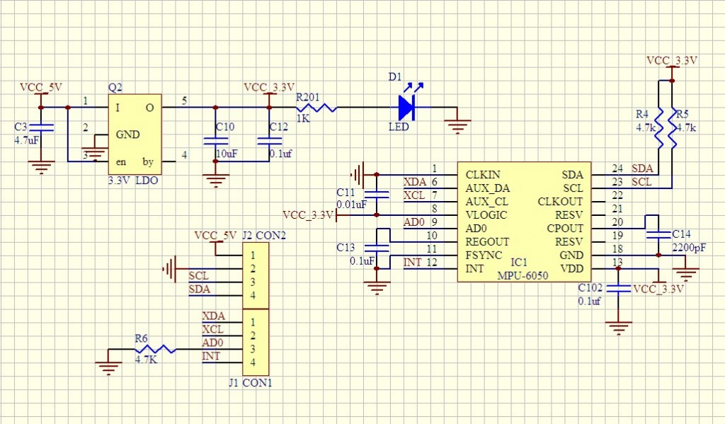
Yes the GY-521 has built in 4.7K pull-ups to 3.3V on SDA/SCL. See https://courses.cs.washington.edu/cours … 24×599.jpg for a reference to R4/R5 pull-ups.
Things work as expected when PPM is not driving PB6.
George
// --------------------------------------

// i2c_scanner

//

// Version 1

//    This program (or code that looks like it)

//    can be found in many places.

//    For example on the Arduino.cc forum.

//    The original author is not know.

// Version 2, Juni 2012, Using Arduino 1.0.1

//     Adapted to be as simple as possible by Arduino.cc user Krodal

// Version 3, Feb 26  2013

//    V3 by louarnold

// Version 4, March 3, 2013, Using Arduino 1.0.3

//    by Arduino.cc user Krodal.

//    Changes by louarnold removed.

//    Scanning addresses changed from 0...127 to 1...119,

//    according to the i2c scanner by Nick Gammon

//    http://www.gammon.com.au/forum/?id=10896

// Version 5, March 28, 2013

//    As version 4, but address scans now to 127.

//    A sensor seems to use address 120.

//

// This sketch tests the standard 7-bit addresses

// Devices with higher bit address might not be seen properly.

//
/* Example pinmap for Bluepill I2Cs (by Testato)
I2C-1 standard pins: PB7(sda) PB6(scl)
Use it by "Wire" without pin declaration
Wire.begin();
I2C-1 alternative pins: PB9(sda) PB8(scl)
Remap the first I2C before call begin()
Wire.setSDA(PB9);
Wire.setSCL(PB8);
Wire.begin();
I2C-2: PB11(sda) PB10(scl)
Remap the second I2C before call begin()
Wire.setSDA(PB11);
Wire.setSCL(PB10);
Wire.begin();
If you want to use the two I2Cs simultaneously, create a new instance for the second I2C
TwoWire Wire2(PB11,PB10);
Wire2.begin();
*/
#include "stm32yyxx_ll.h"
#include <Wire.h>
const uint32_t SDA_PIN = GPIO_PIN_9;
const uint32_t SCL_PIN = GPIO_PIN_8;
void setup() {
GPIO_InitTypeDef GPIO_InitStruct;
pinMode(PB0, OUTPUT);
Serial.begin(115200);
//delay(3000);
Serial.print("RCC->APB2ENR: "); Serial.print(RCC->APB2ENR, HEX); Serial.print(", "); Serial.println(RCC->APB2ENR, BIN);
Serial.print("AFIO->MAPR: "); Serial.print(AFIO->MAPR, HEX); Serial.print(", "); Serial.println(AFIO->MAPR, BIN);
Serial.print("GPIOB->CRL: "); Serial.print(GPIOB->CRL, HEX); Serial.print(", "); Serial.println(GPIOB->CRL, BIN);// Wire.setSDA(PB9);
Serial.print("I2C1->CR1: "); Serial.println(I2C1->CR1, HEX);
Serial.print("I2C1->SR2: "); Serial.println(I2C1->SR2, HEX);
Serial.println();
Wire.setSDA(PB9);
Wire.setSCL(PB8);
Wire.begin();
Serial.print("RCC->APB2ENR: "); Serial.print(RCC->APB2ENR, HEX); Serial.print(", "); Serial.println(RCC->APB2ENR, BIN);
Serial.print("AFIO->MAPR: "); Serial.print(AFIO->MAPR, HEX); Serial.print(", "); Serial.println(AFIO->MAPR, BIN);
Serial.print("GPIOB->CRL: "); Serial.print(GPIOB->CRL, HEX); Serial.print(", "); Serial.println(GPIOB->CRL, BIN); Serial.println("\nI2C Scanner");
Serial.print("I2C1->CR1: "); Serial.println(I2C1->CR1, HEX);
Serial.print("I2C1->SR2: "); Serial.println(I2C1->SR2, HEX);
Serial.println();
/*
//I2C_ClearBusyFlagErrata_2_14_7();
Wire.begin();
Serial.print("RCC->APB2ENR: "); Serial.print(RCC->APB2ENR, HEX); Serial.print(", "); Serial.println(RCC->APB2ENR, BIN);
Serial.print("AFIO->MAPR: "); Serial.print(AFIO->MAPR, HEX); Serial.print(", "); Serial.println(AFIO->MAPR, BIN);
Serial.print("GPIOB->CRL: "); Serial.print(GPIOB->CRL, HEX); Serial.print(", "); Serial.println(GPIOB->CRL, BIN); Serial.println("\nI2C Scanner");
Serial.print("I2C1->CR1: "); Serial.println(I2C1->CR1, HEX);
Serial.print("I2C1->SR2: "); Serial.println(I2C1->SR2, HEX);
Serial.println();
*/
}
void loop() {
byte error, address;
int nDevices;
Serial.println("Scanning...");
Serial.println();
nDevices = 0;
for(address = 0x67; address < 0x69; address++) {
// i2c_scanner uses return value of Write.endTransmisstion to see if device did an acknowledge to address.
Wire.beginTransmission(address);
error = Wire.endTransmission(true);
// I2C1 register dump
Serial.print("- Scan of 0x"); Serial.println(address, HEX);
Serial.print("I2C1->CR1: "); Serial.println(I2C1->CR1, HEX);
Serial.print("I2C1->CR2: "); Serial.println(I2C1->CR2, HEX);
Serial.print("I2C1->OAR1: "); Serial.println(I2C1->OAR1, HEX);
Serial.print("I2C1->OAR2: "); Serial.println(I2C1->OAR2, HEX);
Serial.print("I2C1->DR: "); Serial.println(I2C1->DR, HEX);
Serial.print("I2C1->SR1: "); Serial.println(I2C1->SR1, HEX);
Serial.print("I2C1->SR2: "); Serial.println(I2C1->SR2, HEX);
Serial.print("I2C1->CCR: "); Serial.println(I2C1->CCR, HEX);
Serial.print("I2C1->TRISE: "); Serial.println(I2C1->TRISE, HEX);
Serial.print("RCC->APB2ENR: "); Serial.print(RCC->APB2ENR, HEX); Serial.print(", "); Serial.println(RCC->APB2ENR, BIN);
Serial.print("AFIO->MAPR: "); Serial.print(AFIO->MAPR, HEX); Serial.print(", "); Serial.println(AFIO->MAPR, BIN);
Serial.print("GPIOB->CRL: "); Serial.print(GPIOB->CRL, HEX); Serial.print(", "); Serial.println(GPIOB->CRL, BIN);
if (error == 0) {
Serial.print("I2C device found at address 0x");
if (address < 16)
Serial.print("0");
Serial.println(address, HEX);
nDevices++;
}
else if (error == 4) {
Serial.print("Unknown ERROR at address 0x");
if (address < 16)
Serial.print("0");
Serial.println(address, HEX);
}
Serial.println();
}
if (nDevices == 0)
Serial.println("NO I2C DEVICE FOUND !");
else
Serial.println("done");
Serial.println();
Serial.println("--------");
Serial.println();
delay(2500); // wait 5 seconds for next scan
}
/**
1. Disable the I2C peripheral by clearing the PE bit in I2Cx_CR1 register.
2. Configure the SCL and SDA I/Os as General Purpose Output Open-Drain, High level
(Write 1 to GPIOx_ODR).
3. Check SCL and SDA High level in GPIOx_IDR.
4. Configure the SDA I/O as General Purpose Output Open-Drain, Low level (Write 0 to
GPIOx_ODR).
5. Check SDA Low level in GPIOx_IDR.
6. Configure the SCL I/O as General Purpose Output Open-Drain, Low level (Write 0 to
GPIOx_ODR).
7. Check SCL Low level in GPIOx_IDR.
8. Configure the SCL I/O as General Purpose Output Open-Drain, High level (Write 1 to
GPIOx_ODR).
9. Check SCL High level in GPIOx_IDR.
10. Configure the SDA I/O as General Purpose Output Open-Drain , High level (Write 1 to
GPIOx_ODR).
11. Check SDA High level in GPIOx_IDR.
12. Configure the SCL and SDA I/Os as Alternate function Open-Drain.
13. Set SWRST bit in I2Cx_CR1 register.
14. Clear SWRST bit in I2Cx_CR1 register.
15. Enable the I2C peripheral by setting the PE bit in I2Cx_CR1 register.
**/
#define I2C_PIN_POLL_TIMEOUT 0xFF
//void HAL_I2C_ClearBusyFlagErrata_2_14_7(I2C_HandleTypeDef *hi2c) {
uint32_t I2C_ClearBusyFlagErrata_2_14_7(void) {
uint32_t Timeout = 0;
static uint8_t resetTried = 0;
if (resetTried == 1) {
return 1;
}
GPIO_InitTypeDef GPIO_InitStruct;
// 1. Disable the I2C peripheral by clearing the PE bit in I2Cx_CR1 register.
//LL_I2C_Disable(I2C1);
CLEAR_BIT(I2C1->CR1, I2C_CR1_PE);
// 2. Configure the SCL and SDA I/Os as General Purpose Output Open-Drain, High level (Write 1 to GPIOx_ODR).
GPIO_InitStruct.Pin = SDA_PIN | SCL_PIN;
GPIO_InitStruct.Mode = GPIO_MODE_OUTPUT_OD;
GPIO_InitStruct.Pull = GPIO_NOPULL;
GPIO_InitStruct.Speed = GPIO_SPEED_FREQ_HIGH;
HAL_GPIO_Init(GPIOB, &GPIO_InitStruct);
SET_BIT(GPIOB->ODR, SDA_PIN);
SET_BIT(GPIOB->ODR, SCL_PIN);
// 3. Check SCL and SDA High level in GPIOx_IDR.
Timeout = I2C_PIN_POLL_TIMEOUT;
while ((HAL_GPIO_ReadPin(GPIOB, SDA_PIN) != GPIO_PIN_SET) || (HAL_GPIO_ReadPin(GPIOB, SCL_PIN) != GPIO_PIN_SET)) {
if(Timeout-- == 0) return 1;
}
// 4. Configure the SDA I/O as General Purpose Output Open-Drain, Low level (Write 0 to GPIOx_ODR).
//GPIO_InitStruct.Pin = SDA_PIN;
//HAL_GPIO_Init(GPIOB, &GPIO_InitStruct);
CLEAR_BIT(GPIOB->ODR, SDA_PIN);
// 5. Check SDA Low level in GPIOx_IDR.
Timeout = I2C_PIN_POLL_TIMEOUT;
while (HAL_GPIO_ReadPin(GPIOB, SDA_PIN) != GPIO_PIN_RESET) {
if(Timeout-- == 0) return 1;
}
// 6. Configure the SCL I/O as General Purpose Output Open-Drain, Low level (Write 0 to GPIOx_ODR).
//GPIO_InitStruct.Pin = SCL_PIN;
//HAL_GPIO_Init(GPIOB, &GPIO_InitStruct);
CLEAR_BIT(GPIOB->ODR, SCL_PIN);
// 7. Check SCL Low level in GPIOx_IDR.
Timeout = I2C_PIN_POLL_TIMEOUT;
while (HAL_GPIO_ReadPin(GPIOB, SCL_PIN) != GPIO_PIN_RESET) {
if(Timeout-- == 0) return 1;
}
// 8. Configure the SCL I/O as General Purpose Output Open-Drain, High level (Write 1 to GPIOx_ODR).
//GPIO_InitStruct.Pin = SDA_PIN;
//HAL_GPIO_Init(GPIOB, &GPIO_InitStruct);
SET_BIT(GPIOB->ODR, SCL_PIN);
// 9. Check SCL High level in GPIOx_IDR.
Timeout = I2C_PIN_POLL_TIMEOUT;
while (HAL_GPIO_ReadPin(GPIOB, SCL_PIN) != GPIO_PIN_SET) {
if(Timeout-- == 0) return 1;
}
// 10. Configure the SDA I/O as General Purpose Output Open-Drain , High level (Write 1 to GPIOx_ODR).
SET_BIT(GPIOB->ODR, SDA_PIN);
// 11. Check SDA High level in GPIOx_IDR.
Timeout = I2C_PIN_POLL_TIMEOUT;
while (HAL_GPIO_ReadPin(GPIOB, SDA_PIN) != GPIO_PIN_SET) {
if(Timeout-- == 0) return 1;
}
// 12. Configure the SCL and SDA I/Os as Alternate function Open-Drain.
GPIO_InitStruct.Pin = SDA_PIN | SCL_PIN;
GPIO_InitStruct.Mode = GPIO_MODE_AF_OD;
HAL_GPIO_Init(GPIOB, &GPIO_InitStruct);
// 13. Set SWRST bit in I2Cx_CR1 register.
SET_BIT(I2C1->CR1, I2C_CR1_SWRST);
// 14. Clear SWRST bit in I2Cx_CR1 register.
CLEAR_BIT(I2C1->CR1, I2C_CR1_SWRST);
// 15. Enable the I2C peripheral by setting the PE bit in I2Cx_CR1 register.
//LL_I2C_Enable(I2C1);
SET_BIT(I2C1->CR1, I2C_CR1_PE);
resetTried = 1;
return 0;
}
void GPIO_WRITE_ODR(GPIO_TypeDef* GPIOx, uint16_t GPIO_Pin) {
GPIOx->ODR |= GPIO_Pin;
}
RCC->APB2ENR: D, 1101

AFIO->MAPR: 0, 0

GPIOB->CRL: 44484443, 1000100010010000100010001000011

I2C1->CR1: 0

I2C1->SR2: 0
RCC->APB2ENR: D, 1101
AFIO->MAPR: 2, 10
GPIOB->CRL: 44484443, 1000100010010000100010001000011
I2C Scanner
I2C1->CR1: 1
I2C1->SR2: 0
Scanning...
- Scan of 0x67
I2C1->CR1: 1
I2C1->CR2: 20
I2C1->OAR1: 4066
I2C1->OAR2: FF
I2C1->DR: CE
I2C1->SR1: 0
I2C1->SR2: 0
I2C1->CCR: A0
I2C1->TRISE: 21
RCC->APB2ENR: D, 1101
AFIO->MAPR: 2, 10
GPIOB->CRL: 44484443, 1000100010010000100010001000011
- Scan of 0x68
I2C1->CR1: 1
I2C1->CR2: 20
I2C1->OAR1: 4066
I2C1->OAR2: FF
I2C1->DR: D0
I2C1->SR1: 0
I2C1->SR2: 0
I2C1->CCR: A0
I2C1->TRISE: 21
RCC->APB2ENR: D, 1101
AFIO->MAPR: 2, 10
GPIOB->CRL: 44484443, 1000100010010000100010001000011
I2C device found at address 0x68
done
--------
// --------------------------------------

// i2c_scanner

//

// Version 1

//    This program (or code that looks like it)

//    can be found in many places.

//    For example on the Arduino.cc forum.

//    The original author is not know.

// Version 2, Juni 2012, Using Arduino 1.0.1

//     Adapted to be as simple as possible by Arduino.cc user Krodal

// Version 3, Feb 26  2013

//    V3 by louarnold

// Version 4, March 3, 2013, Using Arduino 1.0.3

//    by Arduino.cc user Krodal.

//    Changes by louarnold removed.

//    Scanning addresses changed from 0...127 to 1...119,

//    according to the i2c scanner by Nick Gammon

//    http://www.gammon.com.au/forum/?id=10896

// Version 5, March 28, 2013

//    As version 4, but address scans now to 127.

//    A sensor seems to use address 120.

//

// This sketch tests the standard 7-bit addresses

// Devices with higher bit address might not be seen properly.

//
/* Example pinmap for Bluepill I2Cs (by Testato)
I2C-1 standard pins: PB7(sda) PB6(scl)
Use it by "Wire" without pin declaration
Wire.begin();
I2C-1 alternative pins: PB9(sda) PB8(scl)
Remap the first I2C before call begin()
Wire.setSDA(PB9);
Wire.setSCL(PB8);
Wire.begin();
I2C-2: PB11(sda) PB10(scl)
Remap the second I2C before call begin()
Wire.setSDA(PB11);
Wire.setSCL(PB10);
Wire.begin();
If you want to use the two I2Cs simultaneously, create a new instance for the second I2C
TwoWire Wire2(PB11,PB10);
Wire2.begin();
*/
#include "stm32yyxx_ll.h"
#include <Wire.h>
const uint32_t SDA_PIN = GPIO_PIN_9;
const uint32_t SCL_PIN = GPIO_PIN_8;
void setup() {
GPIO_InitTypeDef GPIO_InitStruct;
pinMode(PB0, OUTPUT);
Serial.begin(115200);
//delay(3000);
Serial.print("RCC->APB2ENR: "); Serial.print(RCC->APB2ENR, HEX); Serial.print(", "); Serial.println(RCC->APB2ENR, BIN);
Serial.print("AFIO->MAPR: "); Serial.print(AFIO->MAPR, HEX); Serial.print(", "); Serial.println(AFIO->MAPR, BIN);
Serial.print("GPIOB->CRL: "); Serial.print(GPIOB->CRL, HEX); Serial.print(", "); Serial.println(GPIOB->CRL, BIN);// Wire.setSDA(PB9);
Serial.print("I2C1->CR1: "); Serial.println(I2C1->CR1, HEX);
Serial.print("I2C1->SR2: "); Serial.println(I2C1->SR2, HEX);
Serial.println();
Wire.setSDA(PB9);
Wire.setSCL(PB8);
Wire.begin();
Serial.print("RCC->APB2ENR: "); Serial.print(RCC->APB2ENR, HEX); Serial.print(", "); Serial.println(RCC->APB2ENR, BIN);
Serial.print("AFIO->MAPR: "); Serial.print(AFIO->MAPR, HEX); Serial.print(", "); Serial.println(AFIO->MAPR, BIN);
Serial.print("GPIOB->CRL: "); Serial.print(GPIOB->CRL, HEX); Serial.print(", "); Serial.println(GPIOB->CRL, BIN); Serial.println("\nI2C Scanner");
Serial.print("I2C1->CR1: "); Serial.println(I2C1->CR1, HEX);
Serial.print("I2C1->SR2: "); Serial.println(I2C1->SR2, HEX);
Serial.println();
//I2C_ClearBusyFlagErrata_2_14_7();
Wire.begin();
Serial.print("RCC->APB2ENR: "); Serial.print(RCC->APB2ENR, HEX); Serial.print(", "); Serial.println(RCC->APB2ENR, BIN);
Serial.print("AFIO->MAPR: "); Serial.print(AFIO->MAPR, HEX); Serial.print(", "); Serial.println(AFIO->MAPR, BIN);
Serial.print("GPIOB->CRL: "); Serial.print(GPIOB->CRL, HEX); Serial.print(", "); Serial.println(GPIOB->CRL, BIN); Serial.println("\nI2C Scanner");
Serial.print("I2C1->CR1: "); Serial.println(I2C1->CR1, HEX);
Serial.print("I2C1->SR2: "); Serial.println(I2C1->SR2, HEX);
Serial.println();
}
void loop() {
byte error, address;
int nDevices;
Serial.println("Scanning...");
Serial.println();
nDevices = 0;
for(address = 0x67; address < 0x69; address++) {
// i2c_scanner uses return value of Write.endTransmisstion to see if device did an acknowledge to address.
Wire.beginTransmission(address);
error = Wire.endTransmission(true);
// I2C1 register dump
Serial.print("- Scan of 0x"); Serial.println(address, HEX);
Serial.print("I2C1->CR1: "); Serial.println(I2C1->CR1, HEX);
Serial.print("I2C1->CR2: "); Serial.println(I2C1->CR2, HEX);
Serial.print("I2C1->OAR1: "); Serial.println(I2C1->OAR1, HEX);
Serial.print("I2C1->OAR2: "); Serial.println(I2C1->OAR2, HEX);
Serial.print("I2C1->DR: "); Serial.println(I2C1->DR, HEX);
Serial.print("I2C1->SR1: "); Serial.println(I2C1->SR1, HEX);
Serial.print("I2C1->SR2: "); Serial.println(I2C1->SR2, HEX);
Serial.print("I2C1->CCR: "); Serial.println(I2C1->CCR, HEX);
Serial.print("I2C1->TRISE: "); Serial.println(I2C1->TRISE, HEX);
Serial.print("RCC->APB2ENR: "); Serial.print(RCC->APB2ENR, HEX); Serial.print(", "); Serial.println(RCC->APB2ENR, BIN);
Serial.print("AFIO->MAPR: "); Serial.print(AFIO->MAPR, HEX); Serial.print(", "); Serial.println(AFIO->MAPR, BIN);
Serial.print("GPIOB->CRL: "); Serial.print(GPIOB->CRL, HEX); Serial.print(", "); Serial.println(GPIOB->CRL, BIN);
if (error == 0) {
Serial.print("I2C device found at address 0x");
if (address < 16)
Serial.print("0");
Serial.println(address, HEX);
nDevices++;
}
else if (error == 4) {
Serial.print("Unknown ERROR at address 0x");
if (address < 16)
Serial.print("0");
Serial.println(address, HEX);
}
Serial.println();
}
if (nDevices == 0)
Serial.println("NO I2C DEVICE FOUND !");
else
Serial.println("done");
Serial.println();
Serial.println("--------");
Serial.println();
delay(2500); // wait 5 seconds for next scan
}
/**
1. Disable the I2C peripheral by clearing the PE bit in I2Cx_CR1 register.
2. Configure the SCL and SDA I/Os as General Purpose Output Open-Drain, High level
(Write 1 to GPIOx_ODR).
3. Check SCL and SDA High level in GPIOx_IDR.
4. Configure the SDA I/O as General Purpose Output Open-Drain, Low level (Write 0 to
GPIOx_ODR).
5. Check SDA Low level in GPIOx_IDR.
6. Configure the SCL I/O as General Purpose Output Open-Drain, Low level (Write 0 to
GPIOx_ODR).
7. Check SCL Low level in GPIOx_IDR.
8. Configure the SCL I/O as General Purpose Output Open-Drain, High level (Write 1 to
GPIOx_ODR).
9. Check SCL High level in GPIOx_IDR.
10. Configure the SDA I/O as General Purpose Output Open-Drain , High level (Write 1 to
GPIOx_ODR).
11. Check SDA High level in GPIOx_IDR.
12. Configure the SCL and SDA I/Os as Alternate function Open-Drain.
13. Set SWRST bit in I2Cx_CR1 register.
14. Clear SWRST bit in I2Cx_CR1 register.
15. Enable the I2C peripheral by setting the PE bit in I2Cx_CR1 register.
**/
#define I2C_PIN_POLL_TIMEOUT 0xFF
//void HAL_I2C_ClearBusyFlagErrata_2_14_7(I2C_HandleTypeDef *hi2c) {
uint32_t I2C_ClearBusyFlagErrata_2_14_7(void) {
uint32_t Timeout = 0;
static uint8_t resetTried = 0;
if (resetTried == 1) {
return 1;
}
GPIO_InitTypeDef GPIO_InitStruct;
// 1. Disable the I2C peripheral by clearing the PE bit in I2Cx_CR1 register.
//LL_I2C_Disable(I2C1);
CLEAR_BIT(I2C1->CR1, I2C_CR1_PE);
// 2. Configure the SCL and SDA I/Os as General Purpose Output Open-Drain, High level (Write 1 to GPIOx_ODR).
GPIO_InitStruct.Pin = SDA_PIN | SCL_PIN;
GPIO_InitStruct.Mode = GPIO_MODE_OUTPUT_OD;
GPIO_InitStruct.Pull = GPIO_NOPULL;
GPIO_InitStruct.Speed = GPIO_SPEED_FREQ_HIGH;
HAL_GPIO_Init(GPIOB, &GPIO_InitStruct);
SET_BIT(GPIOB->ODR, SDA_PIN);
SET_BIT(GPIOB->ODR, SCL_PIN);
// 3. Check SCL and SDA High level in GPIOx_IDR.
Timeout = I2C_PIN_POLL_TIMEOUT;
while ((HAL_GPIO_ReadPin(GPIOB, SDA_PIN) != GPIO_PIN_SET) || (HAL_GPIO_ReadPin(GPIOB, SCL_PIN) != GPIO_PIN_SET)) {
if(Timeout-- == 0) return 1;
}
// 4. Configure the SDA I/O as General Purpose Output Open-Drain, Low level (Write 0 to GPIOx_ODR).
//GPIO_InitStruct.Pin = SDA_PIN;
//HAL_GPIO_Init(GPIOB, &GPIO_InitStruct);
CLEAR_BIT(GPIOB->ODR, SDA_PIN);
// 5. Check SDA Low level in GPIOx_IDR.
Timeout = I2C_PIN_POLL_TIMEOUT;
while (HAL_GPIO_ReadPin(GPIOB, SDA_PIN) != GPIO_PIN_RESET) {
if(Timeout-- == 0) return 1;
}
// 6. Configure the SCL I/O as General Purpose Output Open-Drain, Low level (Write 0 to GPIOx_ODR).
//GPIO_InitStruct.Pin = SCL_PIN;
//HAL_GPIO_Init(GPIOB, &GPIO_InitStruct);
CLEAR_BIT(GPIOB->ODR, SCL_PIN);
// 7. Check SCL Low level in GPIOx_IDR.
Timeout = I2C_PIN_POLL_TIMEOUT;
while (HAL_GPIO_ReadPin(GPIOB, SCL_PIN) != GPIO_PIN_RESET) {
if(Timeout-- == 0) return 1;
}
// 8. Configure the SCL I/O as General Purpose Output Open-Drain, High level (Write 1 to GPIOx_ODR).
//GPIO_InitStruct.Pin = SDA_PIN;
//HAL_GPIO_Init(GPIOB, &GPIO_InitStruct);
SET_BIT(GPIOB->ODR, SCL_PIN);
// 9. Check SCL High level in GPIOx_IDR.
Timeout = I2C_PIN_POLL_TIMEOUT;
while (HAL_GPIO_ReadPin(GPIOB, SCL_PIN) != GPIO_PIN_SET) {
if(Timeout-- == 0) return 1;
}
// 10. Configure the SDA I/O as General Purpose Output Open-Drain , High level (Write 1 to GPIOx_ODR).
SET_BIT(GPIOB->ODR, SDA_PIN);
// 11. Check SDA High level in GPIOx_IDR.
Timeout = I2C_PIN_POLL_TIMEOUT;
while (HAL_GPIO_ReadPin(GPIOB, SDA_PIN) != GPIO_PIN_SET) {
if(Timeout-- == 0) return 1;
}
// 12. Configure the SCL and SDA I/Os as Alternate function Open-Drain.
GPIO_InitStruct.Pin = SDA_PIN | SCL_PIN;
GPIO_InitStruct.Mode = GPIO_MODE_AF_OD;
HAL_GPIO_Init(GPIOB, &GPIO_InitStruct);
// 13. Set SWRST bit in I2Cx_CR1 register.
SET_BIT(I2C1->CR1, I2C_CR1_SWRST);
// 14. Clear SWRST bit in I2Cx_CR1 register.
CLEAR_BIT(I2C1->CR1, I2C_CR1_SWRST);
// 15. Enable the I2C peripheral by setting the PE bit in I2Cx_CR1 register.
//LL_I2C_Enable(I2C1);
SET_BIT(I2C1->CR1, I2C_CR1_PE);
resetTried = 1;
return 0;
}
void GPIO_WRITE_ODR(GPIO_TypeDef* GPIOx, uint16_t GPIO_Pin) {
GPIOx->ODR |= GPIO_Pin;
}
The above investigation above shows that issue happens when I2C peripheral is busy after Init, which should not be the case indeed.
This is put into light in SR2 status after init :
I2C1->SR2: 2
[fpiSTM – Mon Jan 07, 2019 9:39 am] –
Some update from one of my colleague which do not have an account:The above investigation above shows that issue happens when I2C peripheral is busy after Init, which should not be the case indeed.
This is put into light in SR2 status after init :
I2C1->SR2: 2
When I reconnect the jumper and re-run the test I get the following output. You can see that SR2 shows BUSY after the first call, and is cleared after the second call. The SR2 BUSY after the first call is hit or miss based on timing of the PPM stream and the second Wire.begin() call but you get the idea. In each case the second call clears SR2 BUSY.
RCC->APB2ENR: D, 1101

AFIO->MAPR: 0, 0

GPIOB->CRL: 44484443, 1000100010010000100010001000011

I2C1->CR1: 0

I2C1->SR2: 0
RCC->APB2ENR: D, 1101
AFIO->MAPR: 2, 10
GPIOB->CRL: 44484443, 1000100010010000100010001000011
I2C Scanner
I2C1->CR1: 1
I2C1->SR2: 2 <<<< SR2 BUSY after first Wire.begin() call <<<<
RCC->APB2ENR: D, 1101
AFIO->MAPR: 2, 10
GPIOB->CRL: 44484443, 1000100010010000100010001000011
I2C Scanner
I2C1->CR1: 1
I2C1->SR2: 0 <<<< SR2 cleared after second Wire.begin() call <<<<
Scanning...
- Scan of 0x67
I2C1->CR1: 1
I2C1->CR2: 20
I2C1->OAR1: 4066
I2C1->OAR2: FF
I2C1->DR: CE
I2C1->SR1: 0
I2C1->SR2: 0
I2C1->CCR: A0
I2C1->TRISE: 21
RCC->APB2ENR: D, 1101
AFIO->MAPR: 2, 10
GPIOB->CRL: 44484443, 1000100010010000100010001000011
- Scan of 0x68
I2C1->CR1: 1
I2C1->CR2: 20
I2C1->OAR1: 4066
I2C1->OAR2: FF
I2C1->DR: D0
I2C1->SR1: 0
I2C1->SR2: 0
I2C1->CCR: A0
I2C1->TRISE: 21
RCC->APB2ENR: D, 1101
AFIO->MAPR: 2, 10
GPIOB->CRL: 44484443, 1000100010010000100010001000011
I2C device found at address 0x68
done
--------
About :
PB6 pin SCL is being externally driven by my PPM generator
I’m sorry but I’m still confused about the overall PPM usage and its link to I2C.
As I understand it :
– PB6 as input to get PPM waveform – but I actually don’t see from the code provided how this is used
– I2C is remapped to PB8/PB9 so there are no links to PB6 anymore … The PB6 and I2C1 SCL lines are now 2 different pins, so I don’t understand the above point.
One wild guess: do you observe the same behavior if you connect the 5V on PB5 or PB7 instead of PB6 ?
https://www.st.com/content/ccc/resource … 190234.pdf
ex: 2.13.7 I2C analog filter may provide wrong value, locking BUSY flag and preventing master mode entry
STM32F103 unfortunately has several bugs….
Yes I did reference the F1 errata earlier in the thread. If you look at the bottom of my test sketch you can see I implemented the ST recommended workaround and tested it, but this did not fix the issue.
When I get a chance I’ll try it on an F4 board and see if I get same result.
Best Regards,
George
I would still recommend re-evaluating twi.c initialization logic. I think of it as poor practice to initialize the I2C peripheral on default pins PB6/PB7 when they are in their reset state of input-floating, and then subsequently switching then GPIOs over to user defined alternate pins. More so given the known STM32F1 I2C errata issues (this is the official STM32 core after all isn’t it?
Best Regards,
George
Workaround code below:
#if 1

/**I2C1 GPIO Configuration

PB8     ------> I2C1_SCL

PB9     ------> I2C1_SDA

*/

GPIO_InitStruct.Pin = GPIO_PIN_8|GPIO_PIN_9;

GPIO_InitStruct.Mode = GPIO_MODE_AF_OD;

GPIO_InitStruct.Speed = GPIO_SPEED_FREQ_HIGH;

HAL_GPIO_Init(GPIOB, &GPIO_InitStruct);

__HAL_AFIO_REMAP_I2C1_ENABLE();

#endif
  Wire.setSDA(PB9);

Wire.setSCL(PB8);
Wire.begin();
I2C is not initialized before GPIO.
Only the I2C clock are enable.
Maybe this could cause the issue due to hardware issue on STM32F1.
So, it should be fine to test if moving GPIO init before clock activation solved your issue.
I guess the fact pin get 5V on its input leads us into this issue.
One note, why doing this?
  Wire.setSDA(PB9);

Wire.setSCL(PB8);
[fpiSTM – Mon Jan 14, 2019 3:45 pm] –
One note, why doing this?
Wire.setSDA(PB9);
Wire.setSCL(PB8);
[fpiSTM – Mon Jan 14, 2019 7:05 pm] –
Already done this test with a pwm at 5V and 3.3V and as said not reproduced
Hi Frederic,
Could you please describe how in your test setup are you generating the PPM stream and how is it fed into STM32F1?
George
Simply do an analogWrite(pin, 128);


