Recently I’m trying to design a Pulse induction metal detector using maple mini. I already built two detectors using arduino and they work pretty well. Arduino generated only the timings, but the signal was processed by integrators.
Now I want to built DSP detector. You can see the scheme I drew. Unfortunately electronics and programming is only my hobby and there are much things I don’t know. Such detectors have been already built using atmega328p and atmega8. They all use 10 bits of adc. With faster sampling and better resolution maple mini should have even better performance.
Thanks to the O-Scope project I managed to run the ADC in the fastest mode of 0.58uS per sample. You are great guys
I need to process only the positive portion of the pre amp output signal and this is why I will use the rectifier on the scheme. This will protect the ADC from negative voltage. Now my main concern is – what resistor should I put between the pre amp output and the ADC input? I have no an idea what value to put here. Or maybe just leave it as it is now? I will be happy to hear your opinion. Thank you in advance!
Scheme
If the OpAmp is running on a higher voltage e.g. 5v, you need to use a voltage divider ( resistors) in which case you need to look at what current the OpAmp can produce, e.g. can it for example drive 5mA, and if so, perhaps get it to drive 1mA through a resistor divider
The timing constant of the RV1 (mid position) and C10 is something like 0.5us – do you think that that OPAMP used is fast enough for such speeds?
Mind the D6 zener has a “knee” around 3.3V, so you may not get full 3.3V at the ADC input.
I would also change R1 and R2 to 1k to speedup the edges, add 1k from base to emitter of Q6.
And also do not power MapleMini with 12V, plz.. ![]()
I’m not sure why you’d use a zener, it introduces artefacts you may not want.
Also, what does the 1N4148 do, (well apart from stopping the voltage going below zero to the STM32 if you run a dual rail supply
Both those diodes will impact on your readings
It looks like it runs off a single 12V supply. If so, it doesnt look like the output from the OpAmp is going to go below GND.
I’d probably opt for using a resistor divider on the output of the OpAmp.
Pito, I will add resistor between Q6 gate and emiter. Also will change the R1 and R2 as you suggest and will put 1k in series with the ADC input. Thank you!
The timing constant of the RV1 (mid position) and C10 is something like 0.5us – do you think that that OPAMP used is fast enough for such speeds?
I use RV1 to shrink or strech the signal in order to use the whole 0 to 3.3 range of the ADC input. The C10 is here just for filtering. I have no an idea how to calculate its value, but just saw other people put it there and I did the same ![]()
I’m not sure why you’d use a zener, it introduces artefacts you may not want.
Also, what does the 1N4148 do, (well apart from stopping the voltage going below zero to the STM32 if you run a dual rail supply
Both those diodes will impact on your readings
It looks like it runs off a single 12V supply. If so, it doesnt look like the output from the OpAmp is going to go below GND.
Roger, 1N4148 and RV1 together are acting as half wave rectifier. I saw the half wave rectifier in internet and just replicated it there ![]()
The amplifier runs from -12 and +12, this is why i need to “cut” the negative part of the signal somehow. The zener is here just to protect the ADC from voltages higher than 3.6V. I may remove it, because I can control the signal range by adjusting RV1.
And also do not power MapleMini with 12V, plz.. ![]()
Why is that? It is a maple mini from baite and there is a lable on it which states “vin max 15v”. Or it is not really true?
http://forum.arduino.cc/index.php?topic=65712.0
https://www.lammertbies.nl/electronics/ … ector.html
I’ve been thinking about building one for a while, but other commitments keep getting in the way. I’ll be very keen to know how you get on. ![]()
Why is that? It is a maple mini from baite and there is a lable on it which states “vin max 15v”. Or it is not really true?
That depends on which voltage regulator was cheap at the Shenzhen market that day. Some of these boards have a fairly robust regulator, others I wouldn’t trust with more than about 6V input. If in doubt, add another regulator, but I would avoid any kind of buck regulator unless you are willing to do a bit of additional filtering on your supply lines, as it may add high frequency noise in to the signal you are trying to measure.
I will listen to you and pito, and will feed the maple mini with 5V.
I have built 4 pulse induction detectors and I know how they work in details. My main problem now is how to interface the pre amp with the ADC. There is a simple way of cutting the negative part of the signal which have been used in other DSP detectors:

Unfortunately, using the above method, some part of the negative signal still remains uncut. It is usually about -0.7V. I will not going to sample the signal at the portion when it is negative, because there is no valuable information in this portion, but my main concern is if this negative voltage will damage the maple. I don’t know what is the absolute minimum voltage STM32F103CBT6 ADC can handle. I searched the refference manual and all the documents I have found, but there is no answer. Does anyone here knows? If it can handle -0.7V I will use the method from the above picture.
Page 38 – 5.3.1 General operating conditions. I/O characteristics suggests the pins wont be happy with a negative input in excess of -03V so you are going to have to clamp your -0.7V or level shift it somehow.
The RV1 for amplitude regulation is wrong. You have to use an voltage divider for that (but you do not need as the voltage is limited by zener D6).
The RV1 there is just a part of the timing constant RV1C10. Unless you set RV1 so low that the OPAMP will not be able to feed enough current to the RV1.
Mind the output currents of the Opapm could be 20mA max, so double check.
The D3=1n4148 diode at the opamp output works as a simple peak detector with time constant ~RV1C10.
Based on the first schematics, the max peaks ampl at ADC input will be -0.6 to 3V, with time constant of 0.5usecs (1/2piRV1C10). So the pulse will disappear with aprox this time when the opamp output goes to zero. Not sure you would be fast enough to sample such short pulses properly.
Now – what you want actually want to measure??, as it seems to me you are not clear about that..
If you want to sample the “shape” of the pulses you need an ADC with sample rate at least 10x the 1/(pulse_duration).
If you want to detect the peak amplitude of each pulse you need a longer time constant – similar to the 1/frequency of your pulses into the coil and a good timing between shooting the pulse into the coil and sampling that pulse at the output.
If you want to measure the average amplitude of a train of pulses then you may use large timing constant (ie 10-100ms) and measure the average voltage with the ADC without any need for fast adc.
So what you actually want to do? Mind the electronics is about good understanding of the circuitry and using MATH
PS: I see the frequency of your pulses is 650Hz, 70us/1400us.
So the RV1 shall be for example ~10kohm and C10=10-22nF. That gives you aprox 500-1400us time constant and together with the diode D3 it will work as a simple “peak detector”. You would have about 0.1 x timeconstant to sample the peak till the voltage drops significantly at the ADC input (so something like 50-100us). The precise timing depends on the shape of the pulse, however. So an oscilloscope may help.
Again – you have to specify WHAT you want to measure at the output of opamp to decide on proper signal processing approach..
PS: adding the 1k in series with front of the ADC input will limit the clamp current to the lower clamp diode inside the chip to aprox I = -0.6V/1kohm, the clamp diodes are usually rated for I<<5mA.
Page 38 – 5.3.1 General operating conditions. I/O characteristics suggests the pins wont be happy with a negative input in excess of -03V so you are going to have to clamp your -0.7V or level shift it somehow.
ahull, Thank you!
Pito,
The scheme is based on THIS detector. I have done it with arduino instead of PIC and it works really good. Even better from my Whites SurfMaster detector. Now I want to sample directly from the op amp output instead of using integrators to process the signal.
What i changed on the scheme:
-I removed the 78l05. I use -/+12V for the opamp.
-I use the op amp in inverting mode, because it will be easier to process the signal.
-I tried to cut the negative part of the signal.
This is how the signal usually looks:
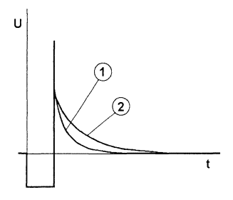
We send a pulse to the ground 1000 times per second. This pulses width is 50uS. Immediately after we stop the pulse, the eddy currents are generating another pulse in the opposite direction. As you can see in the picture this pulse decays slowly for abaout 15uS. This decay forms a curve. If there is no target present, the curve stays the same(there are some small ripples usually). In the picture, 1 is the curve without target and 2 is the curve with some metal target in front of the coil.
What I need to measure is portion of about 15 to 20 uSeconds. The measure should start at the end of the curve. Just before it reaches 0 volts.
How will I measure it: I will “record” about 32 points with convertion speed of 0.58us(Thanks to O-scope project!). Then I will average this 32 points by dividing by 8. In this way I will try to gain 2 extra bits out from the ADC. Then I will average the result with the last 16 results.
All the numbers may be slightly different. I used them just for explanation.
The op amp should have gain of 1000.
NE5534 is exactly 10Mhz and it has a good specs at all. It have been used in many commercial pulse induction detectors.
NE5534 is exactly 10Mhz and it has a good specs at all. It have been used in many commercial pulse induction detectors.
Ok thanks for the explanation on the pulse – that is exactly what we need to know, otherwise just writing mess
The bandwidth BW of an OPAMP depends on the Gain (called BANDWIDTH AT UNITY GAIN), thus 1000x gain and “10MHz bandwidth at GAIN=1” gives you 10kHz bandwidth at gain 1000.
10kHz BW means you can hardly see a 50us pulse.
BTW your gain is set to 500 based on the schematics..
In order to get gain=1000 with a few MHz BW you must use a series of say 3 of your opamps with gain=10 each (thus 1MHZ BW each and in total 1MHz BW, with total GAIN=1000). I doubt there is an OPAMP with GAIN=1000 and real bandwidth=10MHZ at that gain available on the market.. ![]()
Generally, designing amplifiers with such high gains in a single stage is not recommended (for many reasons, especially DC coupled!!).
Also mind the input’s OPAMP offsets will be multiplied by the GAIN too – you must compensate it (with R7 disconnected you have to set the output of the opamp to 0.0V). BTW the input offsets are temperature depended, a coin detected in your lab must not necessarily be detected at -5degC or +35degC in the field..
What you currently measure with your arduino is just an “average of something” at the OPAMP output, which may or may not indicate the golden nugget hidden beneath the coil.. ![]()
PS: below a picture from the simulation:
1. Input -1mV to +1mV, 100us period, 50us pulse, rising/falling edge 1us
2. OPAMP is 70MHz BW, 1000V/usec slew rate, so by far better params than yours
3. GAIN=1000
4. See the output offset +1V due to high gain – must be compensated in your design..
5. The 5pF in your schematics decreases the bandwidth as it creates an low-pass, the corner freq will be aprox 1/(1000k * 5pF) = 200kHz, but it helps with stability a bit..
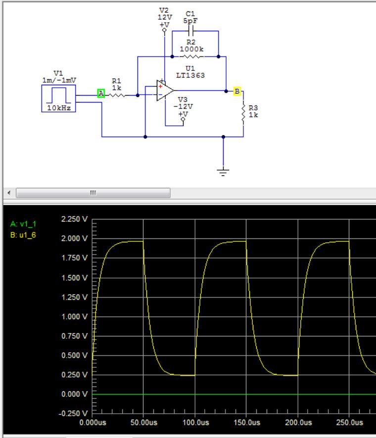
- OPAMP.JPG (67.1 KiB) Viewed 1248 times
- METAL2.JPG (101.53 KiB) Viewed 1244 times
One thing I did not mention is, that the NE5534 have offset compensation circuit. I have build it on my test board, but forgot to draw it in the scheme. This is how it looks http://i.stack.imgur.com/JsIzC.png.
The most important thing I need to know now is how to properly interface it with the ADC.
I will try different configurations and will share the results with you. Unfortunately I have killed my last maple mini and now I have to wait 10 days for the express delivery from China. This time I bough 5 ![]()
“Any” pulse will look like that because you are passing a pulse via a diode and then into an RC, while limiting it with the zener..
So hopefully your new MMs will arrive soon and you may continue!
“Any” pulse will look like that because you are passing a pulse via a diode and then into an RC, while limiting it with the zener..
So hopefully your new MMs will arrive soon and you may continue!
I built it and it works. I generated the tx pulse with arduino nano and the signal after the rectifier looks fine on the real scope.
When my MM arrive I will do more tests and share again 🙂
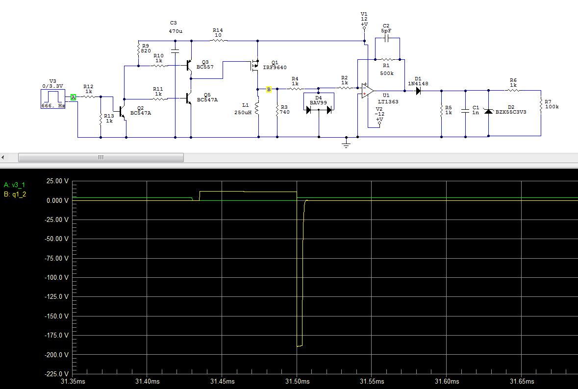
After half a year I finally have some time to play with this metal detector idea. I built it and tried to test it, but there is some problem. As Pito suggested not to feed the Maple Mini from 12V, I put L7805 on the PCB. Here is the SCHEME.
When measuring the L7805 output voltage the multimeter shows 4.95v which seems enough, right? But when I connect the MM the output pulse looks strange:

And there is how the output pulse should actually look. This is with another power supply(5.06v):

I would appreciate any suggestions.
It may happen the current pulse into the coil is so large that your battery drops down to nil volts
Try to switch off the MM from the metal detector circuit and source the MM from USB only. Have a look at the PB1. It must give you a 3.3V pulse.
What O’scope do you use?
I did it. There is no problem from the USB. I also tried from other power supply and still there is no problem. The pulses are 3.3V. The problem occurs only when I feed it from the 7805 of the metal detector’s board.
What Oscope do you use?
It is a cheap “Instrustar ISDS205A” Chinese USB scope. I use it for two years and never had any problems with it.
Now I will test the metal detector board and will write again if there is some progress.
Pito, thank you again for the answers!
The last time I made DIY metal detector it was 30 centimeters deep for a 22mm coin. Not bad for a homemade machine. But it was not DSP and was a lot easyer to do. This time it is hard
The only issue with such setup would be the digging into such deepness – quite an effort
1€ coin – 17cm.
Big gold ring – 21cm.
Tomorow I will play with the damping resistor, the coil and the code and hope to double the depth. Alwso the MM and opamp are put on a socked and not dyrectly soldered to the board. When I solder them I hope to get less noice and better result.
or do you stamp the soil back down ?
srp
or do you stamp the soil back down ?
Yes,I stamp the soil. Anyway disturbed soil affects the test result, but this effect mostly occurs with VLF metal detectors, not with pulse induction.
After one month of using this machine underwater I decided to change the sound frequency, because I can hear better the lower frequencies when underwater. When I closed the box several months ago I put a waterproof connector connected to SWCLK, SWDIO, GND and VCC. It was meant to be used with ST link V2. Today I uploaded the modified code and the sound is now OK, but the LCD does not work anymore. It lights, but characters does not show. Just blank display. I use 16×2 lcd with LiquidCrystal library.
Now when I uploaded the new code with the ST Link I obviously got rid of the bootloader. Maybe this is the reason? Does the LiquidCrystal library needs the bootloader in order to work properly?
I really don’t want to open the box because it is sealed with silicone.
But maybe you changed the GPIO pinout by mistake ?
Of course, you can’t use SWCLK/SWDIO as plain GPIOs…
The LCD is connected as folows:
RS – PC13
E – PC14
D4 – PB4
D5 – PB5
D6 – PB6
D7 – PB7
LED – PA10 (using PWM to adjust)
LED – GND
VO – GND
Looks like I will need to open the damn box ![]()
I saw this thread http://www.stm32duino.com/viewtopic.php?t=1501. Obviously there is some problem with this library when used with ST-Link. In the same thread ahull suggests better not to use JXXX pins. I used PB4 and after reading the ahull’s suggestions I changed it with PA11, but it still does not work.
What is your experience with it after a month? What did you find?
battery flat ?
what doesn’t work, the whole thing, the stm32 or the display(not clear if its that you tested with the nano) ?
does blink work ? maybe you left a blink the led function in the code ? ok you can’t see it, but its only a few mA’s.
to the tone generator for the next time round add a regular ‘i’m still working beep pattern or a ‘i’ve had no input for nn secs” warning one.
have you test code for a nano with any of the hardware ?
can you still separate them to test ?
stephen
[zmemw16 – Sat Jul 22, 2017 8:18 am] –
any signs of leakage?
battery flat ?
what doesn’t work, the whole thing, the stm32 or the display(not clear if its that you tested with the nano) ?
does blink work ? maybe you left a blink the led function in the code ? ok you can’t see it, but its only a few mA’s.
to the tone generator for the next time round add a regular ‘i’m still working beep pattern or a ‘i’ve had no input for nn secs” warning one.
have you test code for a nano with any of the hardware ?
can you still separate them to test ?stephen
Hi Stephen,
The metal detector works except the display. It shows 16 square blocks on the first row for a second and then just a blank display. This is why I tested the LCD with arduino nano. It shows the “Hello word”, so the LCD is working.
There was no signs of leakage in the box. The battery is fully charged. The hardware is OK. The problem occurred after updating the sketch with ST-Link V2.
What is your experience with it after a month? What did you find?
Hi Pito,
I found mostly junk and many coins. Also 4 silver rings and 1 gold earring. I don’t expect to find something valuable, but I enjoy the time spend underwater.
have you a link to it as a project ?
testing the display, literally just the lcd transplanted to a nano already wired for the display?
black blocks and blanks to me suggests the contrast control, did you use a pot ?
stephen
[zmemw16 – Sat Jul 22, 2017 9:44 am] –
how did you program it originally ?
have you a link to it as a project ?testing the display, literally just the lcd transplanted to a nano already wired for the display?
black blocks and blanks to me suggests the contrast control, did you use a pot ?
stephen
1. Originally I programmed it from the mini USB port.
2. I have no link to the project, but I may upload it to my github in the future.
3. Tested the display connected to a nano and it works, so the problem is not in the display itself.
4. There are black blocks only on the first row.
I’m 100% sure the problem is not in the hardware. It is software problem.
Maybe without the bootloader there is no enough time for the LCD to initialize properly. I will try to flash the bootloader back.
After I flashed the bootloader it works again. So if anyone plans to use LiquidCrystal without bootloader, be careful, because it may not work.
you’ve disturbed pin 3 in some way.
what is it wired to, normally its a pot, i suspect you’ve got it going to a pin for maybe pwm ??
5 black blocks and the rest blanks has to be incorrect contrast voltage
change your test for the display to write a char to both lines and all positions ‘hello 7890123456’ ?
i’m expecting you’ll see 30 black blocks and 2 blanks.
i’d run it with the nano as well.
stephen
[zmemw16 – Sat Jul 22, 2017 12:04 pm] –
you’ve beaten me to it, so looks like standard 4bit setup
you’ve disturbed pin 3 in some way.
what is it wired to, normally its a pot, i suspect you’ve got it going to a pin for maybe pwm ??5 black blocks and the rest blanks has to be incorrect contrast voltage
change your test for the display to write a char to both lines and all positions ‘hello 7890123456’ ?
i’m expecting you’ll see 30 black blocks and 2 blanks.
i’d run it with the nano as well.stephen
Pin 3 goes to ground. This LCD requires negative voltage to control the contrast. It looks OK when connected to the ground. On the picture it looks terrible, but it is because of the camera.
[Pito – Sat Jul 22, 2017 1:29 pm] –
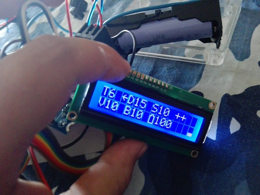
The D15, S10, V10, B10 are the coordinates of the Treasure N.6 (of a large value ++) ?
No, this are the coordinates of a buried big dildo. You can go and dig it up ![]()
How does it work under salty water? Is the signal of the same shape/timing as in the air?
[asen0v – Sat Jul 22, 2017 7:42 am] –
Obviously there is some problem with this library when used with ST-Link. In the same thread ahull suggests better not to use JXXX pins. I used PB4 and after reading the ahull’s suggestions I changed it with PA11, but it still does not work.
Yes, that’s why I told you about pinouts, PB4 is JNRST.
In the file STM32F1/cores/maple/stm32f1/wirish_debug.cpp, you can change the following to allow SW but disable JTAG :
void enableDebugPorts(void) {

//    afio_cfg_debug_ports(AFIO_DEBUG_FULL_SWJ);

afio_cfg_debug_ports(AFIO_DEBUG_SW_ONLY); // Enable SW but still disabling JTAG

}
[martinayotte – Sat Jul 22, 2017 3:38 pm] –[asen0v – Sat Jul 22, 2017 7:42 am] –
Obviously there is some problem with this library when used with ST-Link. In the same thread ahull suggests better not to use JXXX pins. I used PB4 and after reading the ahull’s suggestions I changed it with PA11, but it still does not work.Yes, that’s why I told you about pinouts, PB4 is JNRST.
In the file STM32F1/cores/maple/stm32f1/wirish_debug.cpp, you can change the following to allow SW but disable JTAG :
void enableDebugPorts(void) {

//    afio_cfg_debug_ports(AFIO_DEBUG_FULL_SWJ);

afio_cfg_debug_ports(AFIO_DEBUG_SW_ONLY); // Enable SW but still disabling JTAG

}
Pin 3 goes to ground. This LCD requires negative voltage to control the contrast. It looks OK when connected to the ground. On the picture it looks terrible, but it is because of the camera.
Top
can you post a link to that lcd ?
i have only encountered a negative voltage requirement for a 20×4 lcd, i remember using a 7660 and 2 caps to generate it.
on a standard 16×2 HD44780 interface it normally goes to the wiper of 10k pot connected across the 5v & gnd pins
i use the borne multi-turn ones
stephen
and even
https://www.google.co.uk/url?sa=t&rct=j … rVRUyKpqrg
stephen


All Comments