After evaluating the practicality of this, it does not appear to be economic to produce a F4 board, especially in in BluePill form factor.
The only devices which would fit on such a small board are the F411, which does not provide substantially more processing power than the F103, as its clock speed is only 100Mhz.
The F411 is worse than the F103 for signal acquisition, as it only has 1 ADC (the F103C has 2)
The F405 is a much better processor, but is is not available in a package that would fit on the Blue Pill form factor without using a 4 layer board.
But 4 layer boards as many times more expensive than 2 layers – some PCB plants seem to change 10 times as much for 4 layers.
The other option is to use a BGA version of the F4xx, but these parts are hard to source as they have minimum order quantities of several thousand (probably 1 reel)
And… As has been pointed out by Chris Micro, you can buy a Teensy 3.6 for $19 USD, which is also on a very small form factor, and outperforms most STM32F4 MCU’s
Hence I’m going to park this, as its not worth the time and effort.
_______________________________ Original post ______________________________________
Following form a discussion with @lkcl about creating a STM32 board which is mechanically compatible with the Arduino Due,
http://stm32duino.com/viewtopic.php?f=9&t=2630
the possibility was raised of getting a F4 version of the Blue Pill made by a Chinese manufacturing house.
As the STM32Stamp Eagle design files were published several years ago. ( http://eleccelerator.com/stm32f4stamp-breakout-board/ )
I’ve taken these files and run them though the Eagle2KiCad converter and put the resultant files on Github
https://github.com/rogerclarkmelbourne/ … ill_Boards
In the F405Pill folder
The current status of the files is that the PCB fails DRC because it looks like some vias are not connecting to the filled GND zone on the bottom layer.
I’ve not had chance to figure out why this is happening, and I think perhaps all the via’s to GND may need to be replaced.
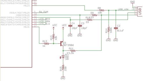
So far I’ve made one change to the schematic, as it looks like the USB D+ was missing the 1.5k pullup to 3.3V that is required by the USB Spec and important if the board has to re-enumerate the USB.
Although the PCB looks good, its wide than the Blue Pill which is a problem on breadboards as there is only 1 row of pins available on each side.
Which makes me wonder if it would be possible to rotate the F405 by 45 deg and perhaps use a 4 layer board for routing – as it would be impossible to route on a 2 layer. However I’m not sure if this would help or worth the additional cost.
The other thing which seems to be making the board wider is are the decoupling caps, and the power LED and its series resistor.
I think that if the LED and resistor are moved, and all the tracks re-routed, the width could be reduced a bit e.g. probably by 0.1 inch at least
If a power LED is needed at all, I’m sure it can be positioned elsewhere
One other omission, seems to be the 32khz crystal. I think there is space on the board for this, and I presume as its low frequency, that the tracks to the crystal don’t need to be ultra short.
- F405Pill.pdf
- (84.56 KiB) Downloaded 81 times
Started out with putting a f303 on it (which is fairly easy to do)
But i’ve also got a bluepill with an F411 on it, and there are also compatible F401, F410, F412 & F413 for it (especially the F413 is ridiculous. 1.5Mb flash, 320kb RAM, and tons of peripherals (but of course you’re still limited to the 36 IO pins…)
the soldering is a PITA, as these are QFN chips, but if you’ve got a hot air station, it’s doable.
And the only other thing you need to do, is put a capacitor on pin 22 (PB11), as on the 4 series it’s an extra capacitor for the internal voltage regulator, and not PB11 (which isn’t present..)
see thread here: viewtopic.php?f=39&t=1658
little extra not (initially?) mentioned in that thread: the bluepill is the only good board to do this on. The maple mini’s pads don’t fit the QFN chips, andn the blackpill is REALLY annoying since it has smd caps right next to the stm32, so changing the stm32 also means you’ll be removing the caps, and then have to get them back on >_<.
- bluepill411.jpg (16.88 KiB) Viewed 3953 times
Thanks
I think perhaps the 41x on the BluePill form factor would be better than the F405 on the larger form factor, as there are plenty of larger F4 boards around.
I just looked on AliExpress, and the F411 is available for $4, no one seems to sell the F413 etc
I’ll have a go at entering what we have for the BluePill schematic into KiCad and post to a different repo
The only sad thing on the f411 is that it only has 1 ADC (so not all pins can do ADC), and no DAC. but it does have i2s (so you can connect a 24 bit I2S dac on it), and a 4 bit SDIO port
1) a reset circuit Maple Mini like or better
2) Power led with solder pad that you can cut to disable for low power.
I was just looking at the schematic symbol in KiCad and I could not find an VDDA (analog supply for ADC I presume) but the 411 doesnt seem have that ![]()
Re: ADC’s
Umm. Thats not so good.
Perhaps the F405 is a better option after all, as I can’t see any of the 64 pin F4’s that have more than 1 ADC (but its really hard to see from STM’s product selector as it doesnt list the actual number of ADC’s in the selector table)
[zoomx – Fri Sep 29, 2017 8:00 am] –
Two suggestions:
1) a reset circuit Maple Mini like or better
2) Power led with solder pad that you can cut to disable for low power.
Reset circuit I think can be a PFET, I think thats what the Seeed Studio Maple clone uses, I’ll try to find their schematis
Re: Power LED
Is it even necessary ?
Also
Boot1 is not really needed, it can be permanently pulled low.
Perhaps it can double as USB DISCONNECT
SIngle transistor USB reset
BTW. I think STM have a single NPN transistor reset circuit on some of their Nucleo’s now.
I’ll see if I can find that… Though I think a PNP may be a better
[RogerClark – Fri Sep 29, 2017 8:12 am] –
@racemaniacI was just looking at the schematic symbol in KiCad and I could not find an VDDA (analog supply for ADC I presume) but the 411 doesnt seem have that
Re: ADC’s
Umm. Thats not so good.Perhaps the F405 is a better option after all, as I can’t see any of the 64 pin F4’s that have more than 1 ADC (but its really hard to see from STM’s product selector as it doesnt list the actual number of ADC’s in the selector table)
All the chips have advantages & disadvantages ^^
I’m happy with the f411 for my projects, but it indeed depends on what you need ![]()
might also one day have a go at drawing out a compact board for a bigger f4 chip with more pins ![]() .
.
[RogerClark – Fri Sep 29, 2017 8:14 am] –
Re: Power LEDIs it even necessary ?
No but in other post I read of it’s presence. If present it’s better ti have a pad to cut.
All low power projects start with cuttin or desoldering the power led, Arduino pro mini and ESP01, for example. TI Launchpads use jumpers but I believe that a simple cutting pad does the work in a cheap board.
OK. That should be easy, just have a track thats easy to cut…
Re: USB enumeration
Rick. So… You’re saying that we don’t need a USB re-enumeration circuit or external 1.5k pullup as its all under SW control ?
https://github.com/rogerclarkmelbourne/ … r/F411Pill
All I’ve done so far is to enter the schematic.
Its currently throwing a load of DRC errors, but this not not unusual for MCUs which have loads of pins, some of which aren’t used.
But I”ll need to double check if any of the errors are valid
I wonder if it may be worth making it 22 pins per side or perhaps 24 pins per side as I think there are more GPIO’s available on the F411 than can be fitted on the 2 x 20 pin connectors.
BTW.
I don’t see any point in having Boot1 on a jump link, as loading into RAM is virtually useless. I guess I could route to a pad in case someone really wants to pull it high, but jump links cost money, and waste space ![]()
[RogerClark – Fri Sep 29, 2017 4:54 am] –
The current status of the files is that the PCB fails DRC because it looks like some vias are not connecting to the filled GND zone on the bottom layer.
after seeing what kind of damage KiCAD can do (long story…), is it ok in Eagle’s DRC?
Which makes me wonder if it would be possible to rotate the F405 by 45 deg and perhaps use a 4 layer board for routing – as it would be impossible to route on a 2 layer. However I’m not sure if this would help or worth the additional cost.
yehhh 2-layer boards particularly ones with only 12mil clearance and tracks, and 12/24-mil VIAs, are extraordinarily low-cost and can be prototyped in 24-48 hours. 4-layer… yyyeah… not worth it.
One other omission, seems to be the 32khz crystal. I think there is space on the board for this, and I presume as its low frequency, that the tracks to the crystal don’t need to be ultra short.
some clean GND tracks surrounding them, and treating XIN and XOUT effectively as diff-pairs… and definitely no VIAs… should be fine.
l.
[racemaniac – Fri Sep 29, 2017 6:15 am] –
the soldering is a PITA, as these are QFN chips, but if you’ve got a hot air station, it’s doable.
the intention for this design is to make use of shenzhen-based component sourcing and assembly, so that people who are in the West can get decent pricing. also as it’s an open board anyone would be able to do assembly themselves (and prototypes too). sigh yes QFNs are a pain… ![]()
[zoomx – Fri Sep 29, 2017 9:36 am] –[RogerClark – Fri Sep 29, 2017 8:14 am] –
Re: Power LEDIs it even necessary ?
No but in other post I read of its presence. If present it’s better ti have a pad to cut.
All low power projects start with cuttin or desoldering the power led, Arduino pro mini and ESP01, for example. TI Launchpads use jumpers but I believe that a simple cutting pad does the work in a cheap board.
are the 32.768 khz XTAL lines likewise potentially useable as GPIO? i remember that being the case on the 072. question is, would people _want_ to use them as GPIO?
[lkcl – Fri Sep 29, 2017 11:27 am] –[RogerClark – Fri Sep 29, 2017 4:54 am] –
The current status of the files is that the PCB fails DRC because it looks like some vias are not connecting to the filled GND zone on the bottom layer.after seeing what kind of damage KiCAD can do (long story…), is it ok in Eagle’s DRC?
As a KiCad user, i’m now wondering what you’re talking about XD
[lkcl – Fri Sep 29, 2017 11:27 am] –
Which makes me wonder if it would be possible to rotate the F405 by 45 deg and perhaps use a 4 layer board for routing – as it would be impossible to route on a 2 layer. However I’m not sure if this would help or worth the additional cost.
yehhh 2-layer boards particularly ones with only 12mil clearance and tracks, and 12/24-mil VIAs, are extraordinarily low-cost and can be prototyped in 24-48 hours. 4-layer… yyyeah… not worth it.
12 mil clearance & tracks seems quite big for something bluepill sized.
i’ve been working 6/6 mil with 24 mil vias, and i think that’s what services like elecrow/dirtypcb/…. support, so also dirtcheap if you go 2 layers. (maybe for some it’s 25 or 27 mil for the vias, not sure, the one i used was ok with 24 mil)
https://pcbshopper.com/
USB disconnect: the MapleMini’s version seems to me the best (2 transistors) as it toggles the 1k5 resistor only if the 5V USB is present. The versions with a single pnp or pfet do not have this option..
Boot1: I am using it (PB2 on BPill) for USB disconnect (pfet). It works fine..
32Khz clock: the RTC’s PC15/14 (BPill) are special pins with lower fanout (see datasheet). The wires to the 32KHz resonator shall be kept short and off the other signals as it is “low” power, thus prone to catch noise.. I think these wires have to have GND guard ring around them..
ADC: mind the agnd/gnd, avcc/vcc topic ![]()
[RogerClark – Fri Sep 29, 2017 10:22 am] –
Re: USB enumeration
Rick. So… You’re saying that we don’t need a USB re-enumeration circuit or external 1.5k pullup as its all under SW control ?
It seems that way, based on information in the reference manual
RM0090 wrote:
34.3.2 Full-speed OTG PHY
The embedded full-speed OTG PHY is controlled by the OTG FS core and conveys USB
control & data signals through the full-speed subset of the UTMI+ Bus (UTMIFS). It provides
the physical support to USB connectivity.
The full-speed OTG PHY includes the following components:
• FS/LS transceiver module used by both host and device. It directly drives transmission
and reception on the single-ended USB lines.
• integrated ID pull-up resistor used to sample the ID line for A/B device identification.
• DP/DM integrated pull-up and pull-down resistors controlled by the OTG_FS core
depending on the current role of the device. As a peripheral, it enables the DP pull-up
resistor to signal full-speed peripheral connections as soon as VBUS is sensed to be at
a valid level (B-session valid). In host mode, pull-down resistors are enabled on both
DP/DM. Pull-up and pull-down resistors are dynamically switched when the device’s
role is changed via the host negotiation protocol (HNP).
• Pull-up/pull-down resistor ECN circuit. The DP pull-up consists of 2 resistors controlled
separately from the OTG_FS as per the resistor Engineering Change Notice applied to
USB Rev2.0. The dynamic trimming of the DP pull-up strength allows for better noise
rejection and Tx/Rx signal quality.
• VBUS sensing comparators with hysteresis used to detect VBUS Valid, A-B Session
Valid and session-end voltage thresholds. They are used to drive the session request
protocol (SRP), detect valid startup and end-of-session conditions, and constantly
monitor the VBUS supply during USB operations.
• VBUS pulsing method circuit used to charge/discharge VBUS through resistors during
the SRP (weak drive).
http://wiki.stm32duino.com/index.php?ti … 7VET6_Mini
http://wiki.stm32duino.com/images/6/69/ … ematic.pdf
it is somewhat explored in an old ‘tiny f4’ thread
viewtopic.php?f=39&t=1977&start=70
among the ‘tiny’ boards there are also various others e.g.
stm32f405rg board from olimex
https://www.olimex.com/Products/ARM/ST/STM32-H405/
and the ‘micro python’ boards (somewhat pricy but fits the compact / tiny definition)
https://store.micropython.org/#/products/PYBv1_1
however all these boards won’t outdo the conventional blue pill or maple mini which slots nicely on a breadboard
that in part as r* and v* chips has lots of pins and if one wants all the pins it would be pretty tough to fit that nicely on a breadboard
Thanks for the links.
I think that breadboard compatibility is quite important, and boards with double rows of pins close to each other are generally hard to use unless you design your own PCB motherboard for your project to use them
The STM32STAMP F405 board is not too bad but its not hardware compatible with the motherboards that people are building to use the BluePill
I think I will try to stick to the BluePill form fator, but this may only be possible if I use a F41x device.
I would consider using a BGA decice, but As far as I can tell they are not any smaller than either the QFLP packages that the F41x or F40x are available in.
Rick.
I will remove the pullup resistor, and add the 32khz osc crystal etc
[racemaniac – Fri Sep 29, 2017 11:58 am] –
As a KiCad user, i’m now wondering what you’re talking about XD
yyeahh… to be honest, if you’ve never tried doing 400 to 600 pin BGA packages on 6 to 8 layer boards, you’ll do absolutely fine. however if you’ve used a proper CAD package which has Design Rules – and i mean *decent* Design Rules… KiCAD is a hell of a shock.
12 mil clearance & tracks seems quite big for something bluepill sized.
i’ve been working 6/6 mil with 24 mil vias, and i think that’s what services like elecrow/dirtypcb/…. support, so also dirtcheap if you go 2 layers. (maybe for some it’s 25 or 27 mil for the vias, not sure, the one i used was ok with 24 mil)
i’ve used eurocircuit’s lowest-possible prototyping service and was really impressed (quality and price). the default rules are… chunky though ![]() good for a 5x7in PCB with only 100-150 components on it. yeah i didn’t realise the bluepill form-factor is really quite tiny, isn’t it? 6 mil should be absolutely fine. if going below 12mil drill hole sizes i’ll have to ask mike’s advice on what’s cheapest.
good for a 5x7in PCB with only 100-150 components on it. yeah i didn’t realise the bluepill form-factor is really quite tiny, isn’t it? 6 mil should be absolutely fine. if going below 12mil drill hole sizes i’ll have to ask mike’s advice on what’s cheapest.
CPU clock speed is listed at 100Mhz, which is not a lot faster than the F103, albeit my be more effecinet per clock, and has FPU
I think I should concentrate on the F405, and try to make it fit the Blue Pill form factor ( though this may be impossible)
I will need to see what physical size the BGA package is, but its got loads of pins ( 176 I think), so its not going to be that small.
So perhaps the Blue Pill form factor is unachieveable ![]()
BTW.
Re: KiCad
I have not had the luxury of using something like Altium so for me, KiCad stacks up very well compared with my 2 year old copy of Eagle ( commercial basic version)
[lkcl – Fri Sep 29, 2017 8:57 pm] –[racemaniac – Fri Sep 29, 2017 11:58 am] –
As a KiCad user, i’m now wondering what you’re talking about XDyyeahh… to be honest, if you’ve never tried doing 400 to 600 pin BGA packages on 6 to 8 layer boards, you’ll do absolutely fine. however if you’ve used a proper CAD package which has Design Rules – and i mean *decent* Design Rules… KiCAD is a hell of a shock.
i have indeed noticed there are a lot of issues with the kicad DRC ^^’
if i look at eagle cad design rule files, there already seem quite some more settings available than what kicad has.
And seeing the push & shove router sometimes still causing violations, or seeing violations reported that don’t seem to make sense, i can imagine that for complex pcb’s, it quickly becomes hell ^^’
The F405RG on its own costs nearly $6 and to squeeze it onto the Blue Pill size board, would require a 4 layer board, with components on both sides of the board (the Blue Pill already has components on both sides, but is a 2 layer board.
So overall, it would probably end up costing at least as much as the larger F405 boards i.e around $10 more than the Blue Pill
I’ll probably put some designs on GitHub for people to check, but I doubt its worth getting a quote to get them manufactured.
[ChrisMicro – Sat Sep 30, 2017 3:49 am] –
Is the performance in the range of a teensy 3.6?
No. Only the expensive F4’s have run at 180Mhz.
I think the price for the Teensy 3.6 would be virtually impossible to complete with.
Its not worth taking this any further as its uneconomic.
I’ve updated the first post and marked this as closed…
[RogerClark – Sat Sep 30, 2017 2:25 am] –
I’m coming to the conclusion, that to get a F405 or F407 onto a form factor which is the same width as the Blue Pill, would probably result in a board costing more than people are willing to pay.The F405RG on its own costs nearly $6 and to squeeze it onto the Blue Pill size board, would require a 4 layer board, with components on both sides of the board (the Blue Pill already has components on both sides, but is a 2 layer board.
https://world.taobao.com/search/search. … TM32F405RG
this is the china-equivalent of ebay so volume pricing may be lower: general offers are around the $3 to $4 mark. does that help?
[lkcl – Sat Sep 30, 2017 7:14 am] –[RogerClark – Sat Sep 30, 2017 2:25 am] –
I’m coming to the conclusion, that to get a F405 or F407 onto a form factor which is the same width as the Blue Pill, would probably result in a board costing more than people are willing to pay.The F405RG on its own costs nearly $6 and to squeeze it onto the Blue Pill size board, would require a 4 layer board, with components on both sides of the board (the Blue Pill already has components on both sides, but is a 2 layer board.
https://world.taobao.com/search/search. … TM32F405RG
this is the china-equivalent of ebay so volume pricing may be lower: general offers are around the $3 to $4 mark. does that help?
Thanks, but the problem is that the 405 simply won’t fit in the Blue Pill form factor ![]()
[RogerClark – Sat Sep 30, 2017 7:21 am] –
Thanks, but the problem is that the 405 simply won’t fit in the Blue Pill form factor
…. won’t fit *at all*… or are you endeavouring to maintain pin-compatibility with the blue pill? the reason i ask it, it was pretty clear from looking at the mega2560 arduino reference design that the entire pinout was designed around… the mega2560. tracks go dead straight, in clear, clean groups, no vias whatsoever. when it came to the 417 (and also the sam3x) the difference is astounding: i’m lucky to have been able to complete the routing *at all*. several areas are a bit… dicey.
so the question in my mind is: are you endeavouring to keep pin-compatibility, because if so yes that would be near-impossible. howeverrr… if creating something that’s pretty much just a break-out board – redefining the pinouts but simply keeping the size – i would be hugely surprised if that didn’t work. and… i’d like this to work ![]()
looking at my breadboards <edit>with a BP plugged in</edit>, one side has 2 holes open, the other 3, i suspect most people could live with 2 + 2.
just checked, had to rummage to find a BP ![]()
minor fly in the ointment, there is good width outside the BP headers to accommodate the silk screen identifiers.
that almost covers inside hole of the pair, using a slightly longer pin length would ease that a lot though.
a really nasty one, use an even long length header and enough force to bend in to fit such that it would be 3 + 3 holes available, or even 4 + 4, if only slight bend desired, increase pcb width by 0.3″ with 2 + 2 holes to use
ok, that’s a tad too far!
something i do with the wide mounting versions of ESP8266 is using 2 breadboards from the SAME source, they are not all created with equal spacing of the locking tabs, or push/pull wire into/from hole resistance; is to reassemble them with a single power bus between the big body parts of the breadboards. P power strip, B main body.
normal is P-B-P-P-B-P, mine P-B-P-B-P, maybe even P-B-P-P-B-P – too wide for ESP8266 – i tried.
be honest, who’s only bought one breadboard ? ![]()
stephen
I could not get a viable routing solution on a 2 later board.
I think it would probably work on a 4 layer board, but the cost of a 4 layer board means no one would buy it, as there would be plenty of cheaper F4 boards which were a different / larger form factor on 2 layers boards.
And as Chris pointed out, the Teensy 3.6 is faster than any F4 MCU I could fit on the Blue Pill form factor and is only $19.
So if anyone wants good performance on a Blue Pill form factor their best option would be to buy a Teensy 3.6
I reason people use the STM32 is because the F103 is dirt cheap and significantly faster than the ATMega328.
If they want more performance and dont need good ADC or DMA etc, then they should probably be looking at the ESP32
[RogerClark – Sun Oct 01, 2017 11:10 am] –
And as Chris pointed out, the Teensy 3.6 is faster than any F4 MCU I could fit on the Blue Pill form factor and is only $19.
30$
19.80$ is the Teensy 3.2 price .
Do i try to break out all pins, or only certain pins? what would the requirements be?
for myself i’d break out the major ports (i2s (= also spi), i2c, uart, …), and whichever other pins are convenient for the format.
i’d try to put an micro sd slot on the pcb (but thus not expose the sdio pins otherwise).
32khz crystal for rtc required or just a nice to have? (how many people actually use it?)
lots of questions ![]()
ideally the size would be small enough to fit 2 of them on a 5x5cm pcb (then at dirtypcb you can have 20 of these boards manufactured for <20$ including slow shipping)
.. I just pointed out that there is the Teensy 3.6 and its performance should be compared to a new BluePill-replacement. I didn’t mention the price.
But I think Paul Stoffregen ( the developer ) put really a lot of effort in his software so he really deserves to make some money with his products.
I was thinking of porting some of his software to the STM32 but I decided not to do it for this reason.
[racemaniac – Mon Oct 02, 2017 2:29 pm] –
i’m going to give it a try to make a 2 layer pcb with a 405 on it, and not too large. lets see how (im?)possible this is.
Do i try to break out all pins, or only certain pins? what would the requirements be?
for myself i’d break out the major ports (i2s (= also spi), i2c, uart, …), and whichever other pins are convenient for the format.
i’d try to put an micro sd slot on the pcb (but thus not expose the sdio pins otherwise).
32khz crystal for rtc required or just a nice to have? (how many people actually use it?)lots of questions
ideally the size would be small enough to fit 2 of them on a 5x5cm pcb (then at dirtypcb you can have 20 of these boards manufactured for <20$ including slow shipping)
I tried to maintain pin compatibility.
It may not be completely impossible on 2 layers, but I think the routing may have to be like a bowl of spaghetti.
The F404 footprint that comes as part of KiCad has a keep-out area under most of the middle of the PCB footprint that does make it impossible to route.
I tried editing the footprint and made the keep-out area smaller so that I could have 2 rows of vias around the inside, but this was not enough to allow it to route.
If the entire middle of the MCU was covered in vias it may help.
Also, if the board extended out beyond the width of the pins it would help, but it would then not fit in a breadboard and have much room to plug pins in around the edge.
I put the files on github in case anyone wants to try this for themselves.
- BluepillF4.zip
- (176.87 KiB) Downloaded 15 times
[RogerClark – Thu Oct 05, 2017 8:38 pm] –
can you post pngs of the top and bottom layers?
you mean like this? (front & back copper layers)

- BluepillF405-F.png (20.92 KiB) Viewed 637 times
I think your tracks are several times smaller than the ones I tried to use.
Edit
Looking at your schematic, I can’t see the two 22R USB protection resistors or the 1.5k pullup
Did I miss something?
Edit.
The 1.5k is not needed but I’m not sure about the 22R
You have vias that partially cover pads for the F405 (I think this may be OK but in most cases the vias could be moved so that they don’t do that)
There seems to be a track shorting power and ground between pins 63 and 64?
Looking at a BluePill I think it has a lot more decoupling capacitors than on your board.
[RogerClark – Thu Oct 05, 2017 10:44 pm] –
Are you using a custom DRC ?You have vias that partially cover pads for the F405 (I think this may be OK but in most cases the vias could be moved so that they don’t do that)
There seems to be a track shorting power and ground between pins 63 and 64?
Looking at a BluePill I think it has a lot more decoupling capacitors than on your board.
the KiCad DRC doesn’t mind vias partially covering pads.
I often do it, but always make sure the drill isn’t too close to the pad (as that’s what causes issues). Heard plenty of advice of preventing the via be in a pad, but slightly touching it?
the board has 6/6 mil tracks/spacing, and 24 mil vias (although reading up on the dirty pcb specs, might have to be 25 mil, but it’s just a quick change)
and there are no shorts. you’re looking at a track leaving pin 64 horizontally i think, there is no short between 63 & 64 (the top plane fill is 3v3, the bottom plane fill is ground)
And i think all required caps etc… are there. but you can have a look at the schematic in the kicad project. it’s just a first try, but seems to be very possible, and i wouldn’t mind using such a board ![]()
i indeed left out the resistors, not sure which is and isn’t needed. Adding them is easy. I tried finding more information about it, but it’s pretty unclear >_<. I think the schematic i found for one of the f4 discovery boards had no resistors at all for the usb.
i’m also wondering if it’s not useful to also connect the ID line to the f4, then it can also be usb host.
[ChrisMicro – Fri Oct 06, 2017 5:49 am] –
Long lives the closed thread
it looks like a fun project ![]()
wouldn’t mind having some of those boards made, and assembling them myself, they seem like fun little things ![]()
might also give it a go to make a more advanced board, not pin compatble, but having a micro sd slot and also breaking out some other pins ![]() .
.
anyone got a clue about what is and isn’t needed in the usb circuits?
checked the f407 discovery board schematic, and it’s got the 22 ohm resistors in series, but it also has this special chip for noise suppresion on usb connected to the line, that also has other resistors in parallel to that, and has some pull up & down resistors >_<
i could always just copy the usb design of the bluepill, it’s not hard adding those resistors below the usb plug.
- BluepillF4v1.0.zip
- (194.62 KiB) Downloaded 21 times

- BluepillF405-F.Cu.png (78.61 KiB) Viewed 797 times
looks good…
Re:Capacitors
The Blue Pill 3.3v rail is quite noisy. I am not sure if the F4 would have the same problems, but if there is space for additional caps, it may be worth adding some more.
I will need to check if the F405 has an analog Vdd input, because if it does, you should have a separate 3.3V reg for that, like the Maple Mini does. The Maple Mini also has a analog Ground input, which is fed though a ferrite core inductor.
The Teensy breaks some pins to pads as its form factor does not have enough through hole pins for all the possible GPIO.
I wonder if there is any space to do the same
[RogerClark – Sun Oct 08, 2017 8:55 pm] –
Re:Capacitors
Yes ! Strongly suggested for any kind of design …
I think its essential to have these separated from the digital Vdd and Vss, as its a major cause of complain with the Blue Pill as it causes poor ADC performance
From what I recall the Maple mini has these but its also a 4 layer PCB. However I know 4 later PCB’s are 10 time the price of 2 layer, so this would need to be achieved on 2 layers.
but it’s indeed not going to be easy
and what would you suggest in extra caps on the voltage regulator?
and i think the bluepill is also noisy because the caps are so nicely organized together in a nice row, rather than placing them close to the pins where the noise would be coming from. look at the caps of its 8mhz crystal for example, their ground pins are on opposite ends of the board, i read that’s pretty bad practice and can thus cause some noise on the ground plane.
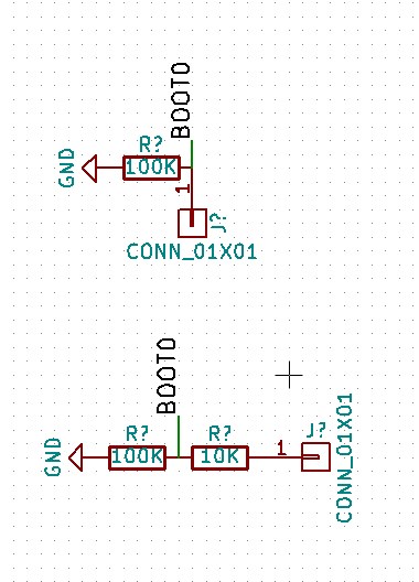
I know that its more practical to load code into RAM on a F4 than it is on a F1 (assuming thats the function of Boot1 on a F4, like it is on a F1).
Or you could put a small solder pad as well as the resistor in case someone really wants to pull Boot1
AFIK, there is a BluePill variant with just the Boot0 jump link.
Regarding the header etc… i also find it overkill. I’d prefer a board with just a pulldown on those pins, and a small pad for if you want to pull them up for those few times you need that.
I’ve also started designing an F4 board that is not pin compatible with a bluepill, but similar in size, and more functionality.
differences:
– the pins a bit further apart (but the board equally wide)
– the board a bit shorter (<5cm)
– a micro sd slot available
– all pins not used by usb/microsd broken out
– als the id pin of the usb connected (so we could be a usb host?)
– no 32k crystal (but maybe i’ll add pads for the capacitors so you can put the crystal between the pins where it should be, and add the capacitors to the pcb).
i’ll also try to give it a dedicated analog supply ![]() .
.
@victor_pv started work on a bootloader for the F4, and its partially working except its not compatible with the existing F1 DFU drivers and we don’t have a way to reset the F4 from the Serial yet etc etc
However I’m sure it would be possible to have bootloader upload for the F4 is we had time to write it
Its just not high priority for anyone
[RogerClark – Mon Oct 09, 2017 9:00 am] –
Some people seem to have Boot0 permanently pulled high during development so that it goes into USB DFU mode for upload.@victor_pv started work on a bootloader for the F4, and its partially working except its not compatible with the existing F1 DFU drivers and we don’t have a way to reset the F4 from the Serial yet etc etc
However I’m sure it would be possible to have bootloader upload for the F4 is we had time to write it
Its just not high priority for anyone
would a default pulldown of the pins, with a header to connect the pin to vcc also be good? (or is there a reason they’re always using a pull up/down rather than directly connecting it).
the bluepill design feels a bit overkill for me ![]() .
.
i think permanent setting boot0 isn’t a good solution after all, on the f407vet black, setting boot zero keeps it jumping to dfu each and every time on reset, no escape.
i think on f4 it can be done in firmware, e.g. detect certain conditions such as a magic sequence, set the software boot0, boo1 registers reboot / reset, into dfu mode. just that i’m not sure how stable this would be,
this would require something like an enhanced upload_reset.exe, which may be a different hassle altogether
the good thing about this ‘trick’ may be that it would stay in dfu mode waiting for the upload after that special reset as that’s what stm32f4’s dfu mode does
the purpose of the board is different: this one contains all someone could need during a project (tft, sdio, rotary encoder, pushbuttons, leds, ecc)
the schematics is quite complete, there are a few notes around. I never started to draw the board since i didn’t had time
to make this i have been taking ideas from maple mini, olimex, nucleo boards, f405 stamp and a few others
features of the board: usb otg, separate analog/digital, Vbat, tft, rotary encoder, sdio, ecc
i wouldn’t be able to work on it until the new year ![]()
Boot1 is also a GPIO pin, so should not be directly connected to GND in case someone accidentally set the pin to High, as it would damage the MCU and potentially affect it booting correctly.
Hence the weak 100k pulldown that gets used.
IMHO Boot0 still needs to be a jumper or potentially a button, but soldering to pads is a pain and can end up lifting tracks off the board if you have to resolder it multiple times.
They will be slightly more expensive, and more difficult to source. They are pretty common on things like hard drives, modern motherboards, set top boxes and the like, so they aren’t that rare.
That board does seem to have the F405 on it, however it must be wider and longer than the Blue Pill, because the only way to get the F405 to fit on the Blue Pill form factor (0.6inch between rows of pins), is to not have the MCU at a 45 deg angle
It seems to have 25 pins down each side, rather than the 20 on the Blue Pill
The price is also quite high (around $15), especially since that a TaoBao price not an inflated AliExpress or eBay price
I think that @racemaniac has done an excellent job fitting the F405 onto the BluePill form factor (assuming his design actually works), and I suspect it would be possible to get it made for under $15 if someone has the right contacts in China
not sure what i’ll do with the boot jumpers, i can probably keep them as is, but i find it a bit overkill for the functionality it provides.
i’ve also been looking into the separate analog power supply, how would you guys see that? you’ve got the 3v3, 5v & gnd pin next to the SWD header, my current idea is to separate them from the rest of the board (also removes that stupid trace i have to do all around the board to get the 5V there), and make that the analog supply.
this does however mean that:
– the only other 5V supply is the usb, so there is no direct pin anymore to connect the 5v to? (maybe put one next to the usb)
– unless you actually have a separate supply, the analog supply will be unpowered unless you connect those pins to something.
but if we really want a completely separate supply, the above is the only option i think. or do we still want to share the 5v & gnd lines between both, and only separate the 3v3 (and give it a separate ground & 3v3 line to the microcontroller with extra decoupling caps for less noise)?
I used part of the maple mini schematic when I investigated if I thought it was possible to produce this board.
Basically, VDD_A needs its own regulator and VSS_A needs a ferrite inductor in series with it.
Looking at the board layout, there is space for the regulator and also probably for the ferrite inductor on the back of the board under the processor, but I don’t know how hard it is to get 5V into that location.
GND would be OK, becuase the processor already has lots of GND pins.
I have tried to open kicad PCB file but there seem to be a some short length of stubs of tracks that don’t seem to go anywhere, which seems strange..
e.g. There is a track on the top / front layer from pin 64 of the F405 , almost tracked to a pad on the back (green) but not via’ed
And there is a separate via, overlaying that pad but not linked to pin 64
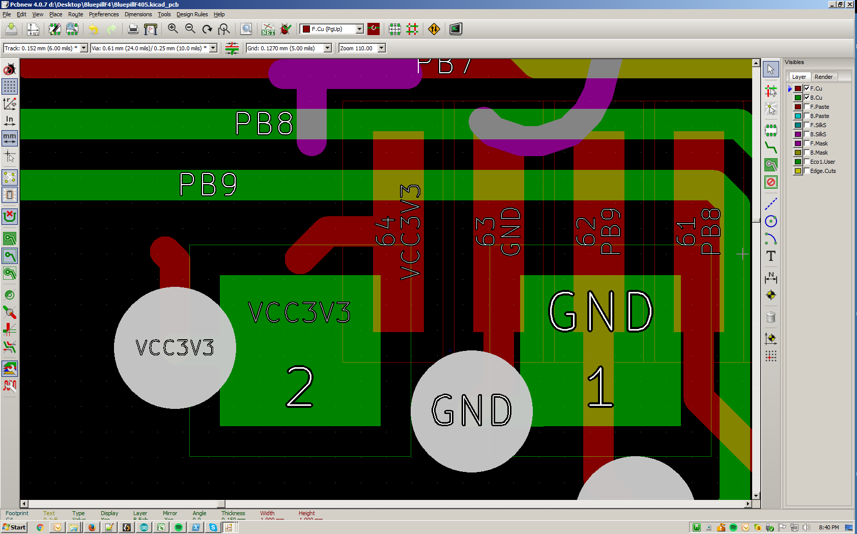
- unattached_tracks.png (112.65 KiB) Viewed 398 times
*edit, checked on my current version of the board (already made some other changes after i posted that version), and it’s okay there ![]() .
.
-option one: a 100k pulldown on it, and a pad connected to it where you can connect it to vcc
-option two: a 100k pulldown, and a 10k pullup with a pad to connect to vcc (as mentioned, boot1 is also an IO, you can’t then short it by connecting it to vcc externally, and putting it to 0 programmatically).
(and for both options, i could also offer vcc pin next to that pin, so not putting the jumper means it’s low, putting it on, means it’s high).
<manager talk> what would be the minimal viable product? </manager talk>
the second option is probably the safest, will work, and if i offer it as a normal pth, you can put a pin on it to connect via a wire to vcc, or solder a wire to it (and remove/solder it back a few times, pth pads aren’t too sensitive).
- boot pin proposals.jpg (50.31 KiB) Viewed 369 times
IMHO … Pulling Boot0 directly to Vcc youself using a wire would not be a serious risk.
I presume you will pull Boot1 low all the time via 100k and not have a jumper.
However I womder if its too minimal if you dont have a pin for Vcc next to the pin for Boot0
Or perhaps a smd push button takes even less space, as its only on one side of the board.
[RogerClark – Tue Oct 10, 2017 6:07 am] –
I think that @racemaniac has done an excellent job fitting the F405 onto the BluePill form factor (assuming his design actually works), and I suspect it would be possible to get it made for under $15 if someone has the right contacts in China
yep i can do that. i’ll need the following:
* clear and complete BOM in TSV format, with a digikey column (helps my friend to make sure his suppliers have got exactly the right part. they don’t buy *from* digikey… they just use the website to make sure the spec’s absolutely correct)
* gerbers including drill-drawing, silk screen, solder mask and paste mask.
* board spec (1.6mm, FR4?), also let me know the min track-to-track, min clearance, and min via drill size.
* how many.
[RogerClark – Tue Oct 10, 2017 6:07 am] –
The price is also quite high (around $15), especially since that a TaoBao price not an inflated AliExpress or eBay price
Right, the price doesn’t compare, that’s why I didn’t save it the first time I saw that board, had to look for the link again.
Hopefully between racemaniac and lkcl something can come out that fits the bill.
[RogerClark – Tue Oct 10, 2017 6:07 am] – I think that @racemaniac has done an excellent job fitting the F405 onto the BluePill form factor (assuming his design actually works), and I suspect it would be possible to get it made for under $15 if someone has the right contacts in China
btw, thanks for the compliment ![]()
i’m pretty sure this board will work (i’ve already made a few iterations of pretty similar lightsaber pcb’s for myself). However, how stable these will be, how to best prevent noise, … i’m still very new to this, so not sure how qualitative all those aspects will be ![]() .
.
But i’m enjoying learning KiCad and making boards like this, so this is a fun project. Once we’ve come to a final design, i’m going to have some produced at dirtypcb’s, and i’ll assemble some for myself to have a look how well these perform (and you guys can give me things to test).
And i’m always all ears for suggestions on things i should mind on the pcb, or how to do certain things better ![]() .
.
It may save a few iterations of getting physical boards and them not quite working
I also noticed that you are using the same regulator footprint as on the BluePill.
From what I can remember, some people complained that those regulators had a habit or turning into firecrackers, but I suppose thats mainly just the current rating.
I looked on my Maple Mini clone and it uses a 3 pad footprint, rather than a 5 pad on the Blue Pill regulator, but I think the overall amount of space consumed on the PCB would be very similar if not exactly the same
[racemaniac – Wed Oct 11, 2017 8:17 pm] –
i’m pretty sure this board will work (i’ve already made a few iterations of pretty similar lightsaber pcb’s for myself). However, how stable these will be, how to best prevent noise, … i’m still very new to this, so not sure how qualitative all those aspects will be.
But i’m enjoying learning KiCad and making boards like this, so this is a fun project. Once we’ve come to a final design, i’m going to have some produced at dirtypcb’s, and i’ll assemble some for myself to have a look how well these perform (and you guys can give me things to test).And i’m always all ears for suggestions on things i should mind on the pcb, or how to do certain things better
it really is exciting, isn’t it? you design something on a computer, and then it comes back as a *real thing* that you spent time on. amazing feeling. anyway. yes. if you’re going to do some prototype assembly in the west it would be better to wait until you have a stable board before asking my friend’s factory in shenzhen to do a quote.
it’s one of the things that i’ve learned, it’s very important not to waste people’s time in shenzhen asking them to run around the markets and suppliers for what can often amount to a few *days* worth of their time… and then they don’t actually receive any money from you. that just pisses them off, and if you’ve asked *someone else* to ask on their behalf (such as my friend, the factory owner), if you do it too many times then *their* reputation goes into the “time-waster” bucket as well.
with things like eurocircuits or other “online” PCB factories (eurocircuits has an absolutely fantastic web site btw), much of the “checking” – the factory rules, DRC compliance and so on – can be done by the web site’s back-end. which is awesome. in china they just don’t have anything like that, it’s all done manually.
so… let’s wait until you have a “final” board design, before getting quotes for 10, 50, 100, 1000, if that’s ok?
It looks like one of the companies I know in China may barter some of my programming effort for building some prototype boards for me if I want.
Nothing definite, but it may be a way to get some prototypes for virtually nothing (apart from my time)
[RogerClark – Thu Oct 12, 2017 12:35 am] –
BTWI also noticed that you are using the same regulator footprint as on the BluePill.
From what I can remember, some people complained that those regulators had a habit or turning into firecrackers, but I suppose thats mainly just the current rating.
I looked on my Maple Mini clone and it uses a 3 pad footprint, rather than a 5 pad on the Blue Pill regulator, but I think the overall amount of space consumed on the PCB would be very similar if not exactly the same
it’s also a 5 pin regulator, but not the same one as the bluepill. The one i’m using is this: AP2112K
i think it’s affordable, and seems pretty ideal for something bluepill like. up to 600mA output current, very low drop off voltage (350mV @600mA, and lowers pretty much linearly with the voltage, so should also be good enough to run this board on Lion cells without having too much of a voltage drop ![]() .
.
[RogerClark – Thu Oct 12, 2017 5:19 am] –
GuysIt looks like one of the companies I know in China may barter some of my programming effort for building some prototype boards for me if I want.
Nothing definite, but it may be a way to get some prototypes for virtually nothing (apart from my time)
very cool. let me know if they’re reluctant to spend the time doing component sourcing: i have two contacts who can help there. they’d both need paying, but… ![]()
Its all dependant on whether their client decides to give them the dev work, and at the moment I’m not convinced that would definitely happen.
[lkcl – Thu Oct 12, 2017 1:24 am] –
so… let’s wait until you have a “final” board design, before getting quotes for 10, 50, 100, 1000, if that’s ok?
… btw racemaniac, just to clarify: i’ve seen various hints that if you happen to have the wrong kicad libraries (or the wrong version or just a different version of kicad) you get a completely different output, and of course you can’t see my screen so wouldn’t be able to check. so when i said “when you’re ready send me the gerbers” that was not me being “lazy” (why would i ask you to send me the gerbers when this is an open project and i could just… download the source and generate them myself, right?) it was so that after all the verification and checking that you’ll be doing, you can *guarantee* – because gerbers are a one-way fixed output – that what you send me will be what you get from the factory. does that make sense?
and strange that my libraries are wrong, i’m on the latest stable of KiCad i think, and normally everything remains up to date (except for the 3d models ^^’)
but if there’s something i can do about the libraries, let me know
and this weekend i’ll have some more time to work on this, let’s see where we can get
I’ll double check what error I got, but from what I remember the schematic editor seemed to have problems with 2 of the symbols and potentially did some replacements
I think potentially the F405 symbol was different, as the one you are using looks nothing like the one that is in the STM32 libraries supplied with KiCad.
When I updated you schematic to add another regulator for Vdd_A, when I read the updated netlist into the PCB editor, it seemed to replace the footprint of the F405 as if it was a completely new component, and I had to move the footprint into the correct location on the PCB, where you had previously routed all the tracks
So I would be a bit concerned about generating gerbers without double checking what was happening with the footprints
[RogerClark – Fri Oct 13, 2017 5:25 am] –
@racemaniacI’ll double check what error I got, but from what I remember the schematic editor seemed to have problems with 2 of the symbols and potentially did some replacements
I think potentially the F405 symbol was different, as the one you are using looks nothing like the one that is in the STM32 libraries supplied with KiCad.
When I updated you schematic to add another regulator for Vdd_A, when I read the updated netlist into the PCB editor, it seemed to replace the footprint of the F405 as if it was a completely new component, and I had to move the footprint into the correct location on the PCB, where you had previously routed all the tracks
So I would be a bit concerned about generating gerbers without double checking what was happening with the footprints
Ah, in the schematic i’m indeed using custom libraries. i usually just quickly make my own lib when needing a component, it’s often faster than hunting down an “official” one
but for the pcb i think the files are completely self describing, so that one should show correctly i think?
but i still find it strange, i thought that was the entire purpose of the BluepillF405-cache.lib : the project stores the versions of the libs it uses in there, and no matter if later on they changed or got removed, it’s in that cache file?
ah well, typical open source stuff i guess XD
On KiCad, if you open a project for viewing it will use cached library data, even if it warns about missing libraries (behaviour may depend on version). However, if you modify the project KiCad may reload data from locally installed libraries, which are usually different to the original ones used.
I had a quick look at the recent zip version, it looked ok. If you have a final version, I could order some boards and hand assemble some prototypes.
this weekend i’ll make all current requested changes, and go for a first “final version”, but expecting more changes to be needed XD.
[RogerClark – Fri Oct 13, 2017 5:25 am] –
@racemaniacI’ll double check what error I got, but from what I remember the schematic editor seemed to have problems with 2 of the symbols and potentially did some replacements
The 2 missing schematic symbols I think are ok, KiCad finds them in the cache lib (worked for me anyways).
When I updated you schematic to add another regulator for Vdd_A, when I read the updated netlist into the PCB editor, it seemed to replace the footprint of the F405 as if it was a completely new component, and I had to move the footprint into the correct location on the PCB, where you had previously routed all the tracks
So I would be a bit concerned about generating gerbers without double checking what was happening with the footprints
There is a small discrepancy, in the schematic the F405 is “U1”, in the PCB it is called “STM32”. I would rename the footprint in the PCB, then it should match the netlist.
[bobc – Fri Oct 13, 2017 11:21 am] –
When I updated you schematic to add another regulator for Vdd_A, when I read the updated netlist into the PCB editor, it seemed to replace the footprint of the F405 as if it was a completely new component, and I had to move the footprint into the correct location on the PCB, where you had previously routed all the tracksSo I would be a bit concerned about generating gerbers without double checking what was happening with the footprints
There is a small discrepancy, in the schematic the F405 is “U1”, in the PCB it is called “STM32”. I would rename the footprint in the PCB, then it should match the netlist.
indeed ^^’ (did it to have the nice STM32 label on the pcb) (could have also just hidden the reference and added it as text XD, or also renamed the reference in the schematic XD)
[bobc – Fri Oct 13, 2017 11:37 am] –
Would it help if I put together a BOM with Digikey part numbers?
can indeed also be helpful
pretty early in this post i already put aliexpress links of the more uncommon components i was using (voltage regulator, usb connector, …)
Digikey parts can also be useful (although for things like the usb connector i hope it’s some fairly standard thing XD. it’s micro usb connector i bought of aliexpress and that seems to be easy to find. made my own custom footprint for it that seems to work well)
[bobc – Fri Oct 13, 2017 12:20 pm] –
Ok, I looked up those links, the reset button I can’t view (account not authorized). For USB Micro, it’s a bit difficult to work with no brand/no part number and the footprints vary a lot. I will probably replace that with something I can order locally.
oops ![]()
here’s a correct link for the button: https://www.aliexpress.com/item/50pcs-3 … 05991.html
chose that one because i had it on hand, and doesn’t require too much space on the pcb, but if there’s a better one to use, that always possible ![]()
[bobc – Fri Oct 13, 2017 12:20 pm] –
Ok, I looked up those links, the reset button I can’t view (account not authorized). For USB Micro, it’s a bit difficult to work with no brand/no part number and the footprints vary a lot. I will probably replace that with something I can order locally.
just… don’t get caught out by using stuff that’s *only* available on digikey. sometimes parts end up being ordered like… 10 years ago by a huge customer, digikey stocks 100,000 of them, then it goes EOL and the *only* place left *in the world* with the parts is… digikey. or avnet etc. etc. it may sound mad but my friend mike has often had people design stuff in the US, sending him a BOM and gerbers and expecting him to be able to just… find everything. he has to explain to them that some parts have to be *imported back in to China*!!
as a general rule though if it’s a very common part, chances are that there will be multiple suppliers, and the vendors know what’s compatible and who to get it from without you needing to specify exactly which random china supplier happens to have it. if you just put in the digikey P/Ns my friend’s suppliers use it to cross-reference and look up a suitable identical part. you would be absolutely amazed: some of them memorise 5 to 10,000 parts including a full current price-list. incredible.
[racemaniac – Fri Oct 13, 2017 12:24 pm] –[edit: do you know if that part is EOL? are there any other suppliers? where would we expect to get more from? what happens if that supplier doesn’t bother responding to enquiries any more?][bobc – Fri Oct 13, 2017 12:20 pm] –
Ok, I looked up those links, the reset button I can’t view (account not authorized). For USB Micro, it’s a bit difficult to work with no brand/no part number and the footprints vary a lot. I will probably replace that with something I can order locally.oops
here’s a correct link for the button: https://www.aliexpress.com/item/50pcs-3 … 05991.html
chose that one because i had it on hand, and doesn’t require too much space on the pcb, but if there’s a better one to use, that always possible
sigh no datasheet, no manufacturer, no part number. pain in the ass to source and find. that would require a trip to Huaqiang Rd markets, to show someone there the photos and ask them to identify it.
bottom line: don’t do it. use something that’s got a part number and manufacturer, like this one:
SKHMQKE010. ALPS Tactile Switch 6.2×6.5×3.1mm SMT
http://www.alps.com/prod/info/E/HTML/Ta … KE010.html
http://eu.mouser.com/ProductDetail/ALPS/SKHMQKE010/
[bobc – Fri Oct 13, 2017 11:37 am] –
Would it help if I put together a BOM with Digikey part numbers?
YES. or farnell / mouser in a pinch. the sourcing rule is:
* find it on digikey, avnet, farnell or mouser first (doesn’t really matter which)
* check the datasheet for suitability
* then go to aliexpress and taobao and search for the part number.
* if it’s got dozens of suppliers of that EXACT part, without there being piss-take prices, it’s good.
if instead you do the following i will NOT help you, because i know it will require several WEEKS of pissing about and possibly actually having to go personally down to the Huaqiang Rd markets, which will mean i have to apply for a 5-day Shenzhen visa, pay for a flight to HK and so on.
* make random arbitrary searches on aliexpress
* don’t provide part numbers, manufacturers, or datasheets
basically whilst the Futian District market suppliers may actually have the full datasheets, their internet access is so piss-poor that they maintain them in an offline fashion ONLY, storing them on laptops and PCs in the tiny 1.2 x 1.5m booths that they actually have to climb over the half-inch thick reinforced glass counters to get in and out of.
so if you want their help you have to email them (in chinese), or you have to go down there personally and show them pictures or actual parts. i apologise but knowing how long that would take, i’m not going to do it (or pay someone else to do it). so please, KEEP THE BOM TO DIGIKEY / MOUSER / FARNELL parts ONLY then check their availability / pricing on aliexpress / taobao, ok? learned that one a long, long time ago.
[lkcl – Fri Oct 13, 2017 1:09 pm] –[racemaniac – Fri Oct 13, 2017 12:24 pm] –[bobc – Fri Oct 13, 2017 12:20 pm] –
Ok, I looked up those links, the reset button I can’t view (account not authorized). For USB Micro, it’s a bit difficult to work with no brand/no part number and the footprints vary a lot. I will probably replace that with something I can order locally.oops
here’s a correct link for the button: https://www.aliexpress.com/item/50pcs-3 … 05991.html
chose that one because i had it on hand, and doesn’t require too much space on the pcb, but if there’s a better one to use, that always possiblesigh no datasheet, no manufacturer, no part number. pain in the ass to source and find. that would require a trip to Huaqiang Rd markets, to show someone there the photos and ask them to identify it.
bottom line: don’t do it. use something that’s got a part number and manufacturer, like this one:
SKHMQKE010. ALPS Tactile Switch 6.2×6.5×3.1mm SMT
http://www.alps.com/prod/info/E/HTML/Ta … KE010.html
http://eu.mouser.com/ProductDetail/ALPS/SKHMQKE010/
It depends on what your requirements are ![]() . For me those are parts i see tons of on aliexpress, and making my own footprint in KiCad once i have one of them isn’t much work (scan it in, put the pads & holes in the right places, and add a few lines to show its size), so that’s why i went for those
. For me those are parts i see tons of on aliexpress, and making my own footprint in KiCad once i have one of them isn’t much work (scan it in, put the pads & holes in the right places, and add a few lines to show its size), so that’s why i went for those ![]() .
.
Depending on who wants to make these boards, it can indeed be required to change those components to something they can easily source, but for my requirements, those were good parts ![]() .
.
but indeed, trying to find those items on digikey will be hard >_<. but it’s only the button & usb connector that will be annoying in that respect, all the other things are standard, so we can always in a later stage change those to whatever fits our requirements ![]() .
.
[racemaniac – Fri Oct 13, 2017 1:23 pm] –
but indeed, trying to find those items on digikey will be hard >_<. but it’s only the button & usb connector that will be annoying in that respect, all the other things are standard, so we can always in a later stage change those to whatever fits our requirements
the requirement is to give the BOM and gerbers to a Shenzhen factory, who will then contact Futian district vendors and have all the parts found and ordered in about 3 days flat. if they have to go randomly searching on aliexpress they’ll simply walk away as they have absolutely no time whatsoever for that sort of thing, given that the profit margins and quantities are really really small.
so – please, follow the sourcing advice that i gave in the previous message, ok?
[lkcl – Fri Oct 13, 2017 1:45 pm] –[racemaniac – Fri Oct 13, 2017 1:23 pm] –
but indeed, trying to find those items on digikey will be hard >_<. but it’s only the button & usb connector that will be annoying in that respect, all the other things are standard, so we can always in a later stage change those to whatever fits our requirementsthe requirement is to give the BOM and gerbers to a Shenzhen factory, who will then contact Futian district vendors and have all the parts found and ordered in about 3 days flat. if they have to go randomly searching on aliexpress they’ll simply walk away as they have absolutely no time whatsoever for that sort of thing, given that the profit margins and quantities are really really small.
so – please, follow the sourcing advice that i gave in the previous message, ok?
If one of you guys has experience with making a good selection of button/usb connector, go for it, i’ll use it in the design (both are ideally sturdy and not too big ![]() ).
).
And wouldn’t just blindly picking something from digikey/… be bad? ideally we’d know what the guy in shenzen can easily and cheaply source, and use that ![]() . not some obscure digikey item that he might not even be able to find.
. not some obscure digikey item that he might not even be able to find.
[racemaniac – Fri Oct 13, 2017 2:04 pm] –
If one of you guys has experience with making a good selection of button/usb connector, go for it, i’ll use it in the design (both are ideally sturdy and not too big
And wouldn’t just blindly picking something from digikey/… be bad? ideally we’d know what the guy in shenzen can easily and cheaply source, and use that
that’s why i said, (1) check on digikey and mouser and farnell FIRST (2) THEN check on aliexpress and taobao SECOND.
the reason is very very simple: aliexpress and taobao suppliers completely fail to provide datasheets and proper references, but they’re a good indicator of availability and pricing.
so you use BOTH… but treat aliexpress and taobao as “unreliable”.
- BluepillF4v1.0b.zip
- (207.58 KiB) Downloaded 10 times
[lkcl – Sat Oct 14, 2017 10:43 am] –
Untitled1.jpgare you able to separate these (vertically), moving them apart so that GND can flood-fill between them? i fuss about things like that.
… hang on… those traces go from red to green with nothing in between! you can move the bottom two to green! or… are you using that jump so as to get GND in there? you should be able to get GND in through the use of some stitching VIAs instead – some above the middle red trace and some below. then you could move both those two green traces to *above* the third (top) red one….
it’s the fill that goes around them that’s important, and indeed, the ground has to go between them to get to the top ground pin of the stm32
[lkcl – Sat Oct 14, 2017 10:41 am] –[racemaniac – Sat Oct 14, 2017 5:40 am] –
Ok, i’ll use that one
I’ve become convinced that there is no intersection between the connectors i see on aliexpress and those i see on digikey XD. i found 1 set of connectors that were very close, nearly identical footprints, but you could physically see on the foto’s that they weren’t identical >_<.*sigh* yehhh that’s why it’s safer to find a mass-produced (common) part. if it’s not actually amphenol it’ll be a cloned-version-of-an-amphenol part… good enough
you’ve got a part number and a manufacturer for that reset switch in the BOM, right? (or… does anyone else know who makes it? google image search?)
yup, this is the reset switch: https://www.digikey.be/product-detail/e … ND/2747186
same one as the bluepill i think, and easy to find both on digikey & aliexpress ![]()
[lkcl – Sat Oct 14, 2017 10:38 am] –
looks really neat and tidy for such a damn small board that’s only 2 layer. dang.some suggested mods which will fill in those white areas. red dots are VIAs on the green area, green dots are VIAs on the red area, i made them opposite colours so they stand out. rerouting (blotch, blotch, hand-drawn GIMP…) shown which works around the proposed VIAs. 3 green, 5 red just so you have an exact tally. obviously i don’t know if they’ll actually work, you’ll have to check that. can i also suggest putting some stitching VIAs along the bottom outer edge. you can’t put any on the top edge because there’s tracks running along the top.
only other thing: this isn’t 480mbit/sec USB, is it? the fact that the USB traces aren’t diff-pairs has me concerned. if it’s only USB 1.1 speeds (12mbits/sec) it should be fine, but if it’s USB2 480mbit/sec then that’s going to be radiating noise like buggery, even if they are really short tracks.
copper layers (1).png
i’ll have a look at your routing suggestions, but the places where there is no fill, is usually also places where it doesn’t really matter. if there’s no pin needing the gnd/3v3 near there, going out of your way to get the fill there is kind of stupid ^^’
and it’s indeed just slow usb. for high speed usb it’s a lot more pins & an extra chip to get to those high speeds.
[lkcl – Sat Oct 14, 2017 10:38 am] –
some suggested mods which will fill in those white areas. red dots are VIAs on the green area, green dots are VIAs on the red area, i made them opposite colours so they stand out. rerouting (blotch, blotch, hand-drawn GIMP…) shown which works around the proposed VIAs. 3 green, 5 red just so you have an exact tally. obviously i don’t know if they’ll actually work, you’ll have to check that. can i also suggest putting some stitching VIAs along the bottom outer edge. you can’t put any on the top edge because there’s tracks running along the top.
The top & bottom fill are different, the top is 3v3, the bottom is ground (so both have a nice connection trough the entire board. I think that what you’re proposing would be if both were the same? then you can indeed stitch them together to form an even better ground plane across the board.
i’m making some more improvements to the routing so it’s all even tidier ![]()
also added two more capacitors as the 3v3 pins without ground next to them of the stm32 didn’t have their decoupling cap yet
[racemaniac – Sat Oct 14, 2017 11:36 am] –
yup, this is the reset switch: https://www.digikey.be/product-detail/e … ND/2747186
same one as the bluepill i think, and easy to find both on digikey & aliexpress
aaaawesooome. that makes the difference between a straightforward buying stint (about 2-4 days) and a whole lot of arseing about, email back and forth with lots of translation into chinese in the mix.
[racemaniac – Sat Oct 14, 2017 12:45 pm] –[lkcl – Sat Oct 14, 2017 10:38 am] –The top & bottom fill are different, the top is 3v3, the bottom is ground (so both have a nice connection trough the entire board. I think that what you’re proposing would be if both were the same? then you can indeed stitch them together to form an even better ground plane across the board.
ahh ok – yehyeh what i proposed was if they were both GND.
And as mentioned, added 2 extra caps to the 3v3 pins that have a VCAP next to them (as opposed to a ground on a 103).
And i just checked, if you bridge C8 & C9 (put in a 0 Ohm resistor), this board is also compatible with a f103 chip
one more thing i’m not sure about if we need to specify something is the ferrite bead connecting analog ground with the normal ground. I know 0603 size beads exist, i currently use a 0603 capacitor footprint for that, but don’t know much about the specs of such beads.
I saw the original maple mini also uses a small smd one (probably also 0603), anyone know if/what we should specify for it?
- copper layers.png (107.53 KiB) Viewed 170 times
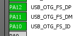
- Not sure I am looking at the latest schematic, but make sure you have PA12 as USB D+ (not PA11!)
- I think the pullup on D+ (R8) is not needed on F405, since there is a pullup internal to the CPU. I would leave the footprint for other devices, but mark it “no fit” for F405.
- If R8 is required, it should pull up to 3.3V, not 5V.
[bobc – Sat Oct 14, 2017 3:00 pm] –
Looks good
- Not sure I am looking at the latest schematic, but make sure you have PA12 as USB D+ (not PA11!)
- I think the pullup on D+ (R8) is not needed on F405, since there is a pullup internal to the CPU. I would leave the footprint for other devices, but mark it “no fit” for F405.
- If R8 is required, it should pull up to 3.3V, not 5V.
thanks for checking everything out, will be correcting those errors ![]() . took the 5V pull up from the bluepill schematic, but i guess that’s wrong then ^^’
. took the 5V pull up from the bluepill schematic, but i guess that’s wrong then ^^’
- BluepillF4v1.0d.zip
- (184.66 KiB) Downloaded 13 times
[racemaniac – Sat Oct 14, 2017 3:56 pm] –
And here is a first go at the BOM:
BluepillF405 BOM.xlsx
I hope xlsx is not a problem for you guys to open?
software libre developer here…. 25 years experience of reverse-engineering and working with embedded systems: i have a tendency to automatically reject proprietary or even non-proprietary file-formats that add a thousand percent or greater overhead, and require applications ten to a hundred thousand times larger than the actual data being viewed. if there’s a choice between “install source code of some program” and “install some f***witt multi-megabyte GUI gunk just for viewing a damn file”… which do you ya think i’m gonna choose? ![]()
also: google the “father sylveste response” regarding presenting people with the unsolicited assumption that you have – or wish to use – vast amounts of computing resources for document viewing and editing. father sylveste is (was?) a jesuit priest who wrote an extremely respectful way of making people aware of the full implications behind *assuming* that sending people arbitrary and proprietary binary-formatted documents is good for the recipient *or the sender*.
short version: gimme TSV or TXT, dude… ![]()
[lkcl – Sat Oct 14, 2017 5:00 pm] –[racemaniac – Sat Oct 14, 2017 3:56 pm] –
And here is a first go at the BOM:
BluepillF405 BOM.xlsx
I hope xlsx is not a problem for you guys to open?software libre developer here…. 25 years experience of reverse-engineering and working with embedded systems: i have a tendency to automatically reject proprietary or even non-proprietary file-formats that add a thousand percent or greater overhead, and require applications ten to a hundred thousand times larger than the actual data being viewed. if there’s a choice between “install source code of some program” and “install some f***witt multi-megabyte GUI gunk just for viewing a damn file”… which do you ya think i’m gonna choose?
also: google the “father sylveste response” regarding presenting people with the unsolicited assumption that you have – or wish to use – vast amounts of computing resources for document viewing and editing. father sylveste is (was?) a jesuit priest who wrote an extremely respectful way of making people aware of the full implications behind *assuming* that sending people arbitrary and proprietary binary-formatted documents is good for the recipient *or the sender*.
short version: gimme TSV or TXT, dude…
as an excel developer i know the basic openxml format of xlsx is open and well documented ^^. (there are some legacy old excel support things in there the libre community complains about, but those are only used in in old documents)
but i’ll provide a csv ![]()
here you go:
- BluepillF405 BOM.csv
- (1.87 KiB) Downloaded 142 times
I think @rikkimball also posted about the USB D+ pullup not being required.
I checked the F4STAMP schematic, and its not present that board, but I think we need to check a few more F4 schematic to be absolutely sure
@racemaniac
Was it impossible to route a pin for the USB OTG ?
Pull-up/pull-down resistor ECN circuit. The DP pull-up consists of 2 resistors controlled
separately from the OTG_FS as per the resistor Engineering Change Notice applied to
USB Rev2.0. The dynamic trimming of the DP pull-up strength allows for better noise
rejection and Tx/Rx signal quality
So it has the pull up resistor, and it controls it by itself.
Another interesting thing, is that pin PA9 can be configured as VBUS monitoring, to detect whether the USB cable is connected or disconnected.
No idea if all the pins are broken out, but if PA9 is not and will be unused, then it would good to connect it to VBUS.
Section 34.5.2 decribes how to control the DP pull-up:
Soft disconnect
The powered state can be exited by software with the soft disconnect feature. The DP pullup
resistor is removed by setting the soft disconnect bit in the device control register (SDIS
bit in OTG_FS_DCTL), causing a device disconnect detection interrupt on the host side
even though the USB cable was not really removed from the host port.
[racemaniac – Sat Oct 14, 2017 5:13 pm] –
as an excel developer i know the basic openxml format of xlsx is open and well documented ^^. (there are some legacy old excel support things in there the libre community complains about, but those are only used in in old documents)
but i’ll provide a csvhere you go: BluepillF405 BOM.csv
star. ok looks pretty simple, doesn’t it. for when that goes to the factory are you able to “group” them so there’s a QTY column and a column listing the references?
11; C1 C2 C3 C4…. ; SMD Capacitor 0.1uF 0603;
4; C5 C6 C10 C11; SMD Capacitor 20pF 0603;
etc. etc.
the ferrite bead, not for any particular reason, i happen to be using this one for an audio circuit, it’s quite beefy for an 0603: 1.2A, and it presents 330 ohms @ 100mhz and has a DCR of under 150mOhm (0.15 ohms).
https://www.digikey.com/product-detail/ … ND/1948327
if anyone else feels that spec’s not appropriate for this task do say so. i’m using an MH2029-300Y (3A rating, 300ohm @ 100mhz) in the stl47o but it’s an 0805.
soo… could someone confirm that this is the right procedure:
* look at the datasheet, get its capacitance value
* subtract 10pF (for the pins/traces inherent capacitance)
* because the capacitors are in series to GND, you use the formula 1/(1/C + 1/C) which happens to equal 2 * C
therefore the complete formula for the xtal capacitors is: (DATASHEET VALUE – 10) * 2
is that correct? so for the 8mhz XTAL it’s 20pF so you need (20-10) * 2 = 20pF
but for the 32.768kHz XTAL it’s 12.5pF so you need (12.5pF – 10) * 2 = 5pF
does that look right? did i miss anything?
[lkcl – Sun Oct 15, 2017 1:37 am] –
btw… the crystals… reading the datasheets, they mention that you should assume 10pF capacitance on pins and traces, and that you have to match the capacitance of the *crystal*, is that right?soo… could someone confirm that this is the right procedure:
* look at the datasheet, get its capacitance value
* subtract 10pF (for the pins/traces inherent capacitance)
* because the capacitors are in series to GND, you use the formula 1/(1/C + 1/C) which happens to equal 2 * Ctherefore the complete formula for the xtal capacitors is: (DATASHEET VALUE – 10) * 2
is that correct? so for the 8mhz XTAL it’s 20pF so you need (20-10) * 2 = 20pF
but for the 32.768kHz XTAL it’s 12.5pF so you need (12.5pF – 10) * 2 = 5pF
does that look right? did i miss anything?
what do we do, reduce the capacitors, or ask for a 32khz crystal that is also 20pF? (they also exists, the blueprint schematic has 20pF capacitors on both crystals, so maybe they have one like that. But looking on aliexpress, they seem to all be 12.5pF)
[RogerClark – Sat Oct 14, 2017 8:21 pm] –
@bobcI think @rikkimball also posted about the USB D+ pullup not being required.
I checked the F4STAMP schematic, and its not present that board, but I think we need to check a few more F4 schematic to be absolutely sure
@racemaniac
Was it impossible to route a pin for the USB OTG ?
shouldn’t be hard, i assume it’s just connecting PA10 to the ident pin? nothing special?
I thought victor said PA9, but perhaps this is not the same thing (and I didnt check the datasheet)
[RogerClark – Sun Oct 15, 2017 7:13 am] –
PA9 or PA10 ??I thought victor said PA9, but perhaps this is not the same thing (and I didnt check the datasheet)
- usb.jpg (12.51 KiB) Viewed 240 times
I wonder what Victor was referring to, or if it was just a typo.
PA10 can be used for ID detection, PA9 for VBUS detection. To support USB host, you need something to switch +5V onto VBUS, which ideally should also provide overcurrent protection.
I note on their design, ST use 20 pF on the 8MHz xtal, and 6.8pF on the 32.768kHz (MC306-G-06Q-32.768, manufacturer JFVNY). I’ve never heard of JFVNY, and couldn’t find a datasheet, so that doesn’t help much!
Edit: found datasheet here http://en.jfvny.com/downloadRepository/ … 9728fd.pdf I know some people try to account for stray capacitance, but I’m not sure if guessing the value without actually measuring it is a good idea. Some people use 5pF as a rule of thumb. I’ve never seen any real measurements which actually show the oscillator is more stable with the “right” value of load capacitor, it’s always a paper exercise. I suspect this is one of those “folklore” things that people like to do but actually has no measureable benefit.
[bobc – Sun Oct 15, 2017 7:42 am] –
I’m using the STMF4DISCOVERY as a reference circuit, http://www.st.com/en/evaluation-tools/s … overy.htmlPA10 can be used for ID detection, PA9 for VBUS detection. To support USB host, you need something to switch +5V onto VBUS, which ideally should also provide overcurrent protection.
I note on their design, ST use 20 pF on the 8MHz xtal, and 6.8pF on the 32.768kHz (MC306-G-06Q-32.768, manufacturer JFVNY). I’ve never heard of JFVNY, and couldn’t find a datasheet, so that doesn’t help much!
mc-306 is what i’m using for footprint now, i’ll switch the values to 6.8pF
and for the VBUS, if anybody has an idea on how to implement that, i’m all ears ![]() . (preferably not taking up too much space XD)
. (preferably not taking up too much space XD)
[racemaniac – Sun Oct 15, 2017 5:39 am] –
what do we do, reduce the capacitors, or ask for a 32khz crystal that is also 20pF? (they also exists, the blueprint schematic has 20pF capacitors on both crystals, so maybe they have one like that. But looking on aliexpress, they seem to all be 12.5pF)
stick with those, then, if they’re commonly available (means lower-prices) and reduce the capacitors to 5pF. does that sound like a good strategy?
[lkcl – Sun Oct 15, 2017 10:25 am] –[racemaniac – Sun Oct 15, 2017 5:39 am] –
what do we do, reduce the capacitors, or ask for a 32khz crystal that is also 20pF? (they also exists, the blueprint schematic has 20pF capacitors on both crystals, so maybe they have one like that. But looking on aliexpress, they seem to all be 12.5pF)stick with those, then, if they’re commonly available (means lower-prices) and reduce the capacitors to 5pF. does that sound like a good strategy?
yup, that’s a deal ![]()
[bobc – Sun Oct 15, 2017 7:42 am] –
I’m using the STMF4DISCOVERY as a reference circuit, http://www.st.com/en/evaluation-tools/s … overy.htmlPA10 can be used for ID detection, PA9 for VBUS detection. To support USB host, you need something to switch +5V onto VBUS, which ideally should also provide overcurrent protection.
i typically use the SY6280 for that, but it’s a SOT23-5 and requires 5 components (resistor-divider for the current, 2 4.7uF and 1 0.1uF capacitors). that’s starting to get quite a lot already.
what you can do is use it like a controllable diode with built-in overcurrent protection.
the other circuit i’ve seen is the one on the arduino and the due, which uses an LM385D. westfw on arduino.cc helped track down an SOT23-5 variant (single Op-Amp) which does the job as well: you put the 3v3 on one of the op-amp inputs (Minus) and VBUS on the other (Plus), then wire the output of the Op-Amp directly to a MOSFET. which you also have to have space for (SOT23-3). actually… just looking at the Due Reference Design they just have *two* MOSFETs, one for USBVCC with the gate wired straight to GND, and the other gate connected to that op-amp. it’s 10 components total. one SOT23-5 (op-amp), three SOT23-3 (MOSFETs and transistor) plus discretes.
it starts to get… well… that’s a lot of extra components for such a small – and busy – board space.
my feeling is: the op-amp, transistor etc. could all be replaced with the SY6280, you probably *already have* 4.7uF power-in/out capacitors in place… and you could keep the trick of having the MOSFET with its gate wired to GND to act as a one-way power “diode”.
Some people use 5pF as a rule of thumb. I’ve never seen any real measurements which actually show the oscillator is more stable with the “right” value of load capacitor, it’s always a paper exercise. I suspect this is one of those “folklore” things that people like to do but actually has no measureable benefit.
ST’s application note, referenced in their various MCU datasheets, explains it well. AN4555 page 24/25 has the formula, and then also mentions how to reduce “stray” capacitance which can be anywhere between 2pF and 7pF, and depends on the board layout *for the decoupling capacitors*… not the *crystal* capacitor layout.
it’s complicated in other words.
nom, nom, nom… shuffle…. XTAL to left of F405 goes over by 0.5mm…. F405 goes over by 1mm…. 4-pin header moves left by 1.5mm but without breaking the power/gnd plane that’s going round it….
… that would definitely give you enough room near the USB connector to drop in a SY6280, the resistor-divider and an SOT23-3 MOSFET. datasheet’s easy to find, google “SY6280 datasheet”.
you *might* be able to get away with just moving the 4-pin header over by abouuuut… 0.5mm and not have to move the F405 or the XTAL.
KiCad and dragging footprints aren’t the best combination >_<
How much current are we expecting this board to draw? the ap2112 is great for operating from a battery, and for low currents, but indeed, it will never stay alive at its 600mA max @5V without proper cooling. probably safe (but hot) up to 200mA @ 5V, but probably not much more. What are our requirements there? do we need to upgrade to an lm1117 (but which has a higher voltage drop, so less suited for battery operation) (basically the same as the AMS1117 i think, also huge voltage drop…).
how much power are we expecting this board to be used for? as is also mentioned in the thread, we can try connecting some of its pins to a plane to provide extra cooling (but which pins would be best >_<)?
*edit*
i’ve just made a test setup with my maple mini that i upgraded with a ap2112. according to my keweisi usb power tester it’s currently getting 270mA @4.6V, and it seems to be holding up pretty well (it’s hot but not burning hot).
According to the datasheet @ those conditions it should be about 63°C (180° per watt without external cooling), i don’t have a thermometer to measure but that seems realistic.
does that seem like a usable voltage regulator for our board, or is it too weak & fragile?
[racemaniac – Sun Oct 15, 2017 12:41 pm] –
How much current are we expecting this board to draw?
the SY6280 copes with switching up to.. 1.5A i think.
F405 moving: disconnect the most immediate tracks then redo them.
[lkcl – Sun Oct 15, 2017 1:07 pm] –[racemaniac – Sun Oct 15, 2017 12:41 pm] –
How much current are we expecting this board to draw?the SY6280 copes with switching up to.. 1.5A i think.
F405 moving: disconnect the most immediate tracks then redo them.
i mean the 3v3 part. just read the documentation of the F405, and it’s rated to draw at most 240mA, + 10mA for the 2 leds, we should be able to handle 250mA.
I think that’s well within reach of a single ap2112 @ 5V. it’ll probably go to 70-80 °C, but that’s acceptable i think as a worst case scenario?
I domder what happens to the USB If serial1 is used.
Does it affect the host PC Serial USB driver etc
[RogerClark – Sun Oct 15, 2017 5:32 pm] –
I just remembered PA10 is part of Serial1I domder what happens to the USB If serial1 is used.
Does it affect the host PC Serial USB driver etc
hmmm… just looking at the datasheet, OTG_FS_ID (PA10) and OTG_HS_ID (PB12) are both “weak pullup” resistors. oh! i think…. i think there’s actually 2 sets of USB OTG interfaces/pins, one set on PA (FS) and one on PB (HS). but you can’t do DFU firmware-flashing through the PB set, only PA11/PA12.
honestly… i feel: if PA10/11 was previously dedicated to USART1_RX, if it doesn’t interfere with interoperability with the bluepull pinouts (i.e. if PA10 can be dedicated to OTG_FS_ID and there’s another couple spare pins with alternative functions as UART TX/RX) i’d say don’t worry about it.
alternative functions for USART1_TX are also on PB7, so if PB7’s not being used that could do the job.
or, USART3 is on PC10/PC11 and also PB10/PB11.
if there’s a priority consideration to use PA10/PA11 for UART-style DFU boot-loading i’d suggest not worrying about that, as USB DFU can take care of that. leave PA10/PA11/PA12 as dedicated to USB, defintely don’t try sharing it.
i’ll try to see if there’s a PDF schematic published somewhere. roger we really need a wiki page for this project, which can keep/manage static links. forums are great for instantaneous narrow-time-window-of-opportunity communication… as long as you keep up-to-date with the discussion…. but they’re a bitch for actually finding useful information. …. remember the AOL “me-too” posting syndrome? ![]()
[racemaniac – Sun Oct 15, 2017 1:17 pm] –
i mean the 3v3 part. just read the documentation of the F405, and it’s rated to draw at most 240mA, + 10mA for the 2 leds, we should be able to handle 250mA.
I think that’s well within reach of a single ap2112 @ 5V. it’ll probably go to 70-80 °C, but that’s acceptable i think as a worst case scenario?
bit high! personally i like staying well below rated currrents if possible….
couple of circuits for you. VBUSDET is on a resistor-divider bridge: it’s a cheap way to not need the op-amp. from the arduino circuit you can substitute the MOSFET and the transistor and the op-amp with the SY6280. keep the MOSFET-with-the-gate-to-GND as the power-in-with-a-builtin-diode. aand… you’re done. third picture is from DOCID022152 page 187 en.DM00037051.pdf, stm32f405xx/407 datasheet.
- Untitled1.jpg (26.42 KiB) Viewed 264 times
okaaay sooOoo…. PC6 and PC7 are spare. they also have TIM function as well as USART6_TX and USART6_RX. however it looks like you’d also need CTS… and there isn’t a USART6_CTS/RTS – not on the 64-pin variant anyway.
honestly…. looking at the original bluepill, they also wired up PA10-PA12 directly to *both* USB *and* the pin-header…. presumably because of the low pin-count…
i think… it’s basically far too complicated to try dedicating pins to UART and pins to USB, do exactly what they did, but put OTG onto the USB header as well… and *as long as* there is no extra components on PA10 (no pullup/pulldown), as long as you rely on the 405’s internal capabilities to implement the OTG_ID pullup/down functionality, you should be fine.
basically if anyone *really wants* to use PA9/PA10 for TX/RX they’ll just have to live with the fact that they can’t do that and have OTG functionality at the same time. they’re getting the *additional possibility* of OTG functionality when compared to the original BluePill, which didn’t have that at all.
But as the main reason for using the BluePill form factor is so that people could use this as a drop in replacement for existing projects which could use more speed / performance. I think its important to keep PA9 and PA10 connected as Serial (USART 1)
I don’t think it matters if USB OTG does not work while using USART 1, but ideally the normal USB connection to a PC (or Mac etc) should still work when PA9 and PA10 (USART 1) are in use.
[racemaniac – Sun Oct 15, 2017 1:17 pm] –[lkcl – Sun Oct 15, 2017 1:07 pm] –[racemaniac – Sun Oct 15, 2017 12:41 pm] –
How much current are we expecting this board to draw?the SY6280 copes with switching up to.. 1.5A i think.
F405 moving: disconnect the most immediate tracks then redo them.
i mean the 3v3 part. just read the documentation of the F405, and it’s rated to draw at most 240mA, + 10mA for the 2 leds, we should be able to handle 250mA.
I think that’s well within reach of a single ap2112 @ 5V. it’ll probably go to 70-80 °C, but that’s acceptable i think as a worst case scenario?
RT9166-33GVL is rated for 300mA. and the RT9166A is even rated for 600 (in a SOT23-3 package!) pricing on taobao is mad – RMB 1 to RMB 0.25 https://s.taobao.com/search?q=RT9166-33GVL
https://www.digikey.com/product-detail/ … ND/2546644
http://www.richtek.com/assets/product_f … 66A-23.pdf
buuut… hmmm. 300mA @ 3.3v = 1 watt and that completely exceeds the rating of 0.4W for the SOT23-3 package. whoops. do you have room for a SOT-223?
hmm just checking the AP2112k-3.3 pricing on taobao and i think it beats the RT96166 by quite a margin. there’s also a 600mA version of it (the 3.3trg1).
*hand-waving*… the AP2112k-TRG1 should be fine. he said.
max rating is 1A, it’s in a proper package with heatsink you can connect to a plane on the board. i’ll have to see if i can make room for it on the board, but i think it’s possible. it will probably make our BOM 0.5$ more expensive, but then we have a voltage regulator that can handle all reasonable cases. for the analog section we can then stick to the ap2112, it’s more than enough for there
and then we still have nice voltage regulators that have a very low voltage drop, so battery operation remains an option
*edit*
maybe this one is the winner
and damn i hate how hard these things are to find on aliexpress. Unless i fully type “AP2114HA”, it shows nothing. AP2114 gives me no results what so ever >_<.
[racemaniac – Mon Oct 16, 2017 6:48 am] –
someone else mentioned the ap2114d, which is a lot more expensive i’m afraid (on aliexpress only 1 dealer, selling per 5, @ 0.6€ a piece), but seems the perfect fit for all we can want
aliexpress remember is targetted at selling abroad. taobao is the internal-to-china-version-of-ebay. use that to check instead ok? like this:
https://s.taobao.com/search?q=AP2114HA-3.3TRG1
so… plenty of suppliers on that one.
max rating is 1A, it’s in a proper package with heatsink you can connect to a plane on the board. i’ll have to see if i can make room for it on the board, but i think it’s possible. it will probably make our BOM 0.5$ more expensive, but then we have a voltage regulator that can handle all reasonable cases. for the analog section we can then stick to the ap2112, it’s more than enough for there ![]() .
.
and then we still have nice voltage regulators that have a very low voltage drop, so battery operation remains an option ![]() .
.
https://s.taobao.com/search?q=RT9166A-33GG
RMB 0.40 dang. but only the one supplier.
https://s.taobao.com/search?q=AP2114D-3.3TRG1
lots of suppliers. RMB 1.50, RMB 2, looks like a good choice.
i think really the TO-252 package is what’s needed: it can clearly handle the current properly and dissipate the heat.
[RogerClark – Mon Oct 16, 2017 4:14 am] –
I didnt expect USB and OTG USB to work at the same timeBut as the main reason for using the BluePill form factor is so that people could use this as a drop in replacement for existing projects which could use more speed / performance. I think its important to keep PA9 and PA10 connected as Serial (USART 1)
I don’t think it matters if USB OTG does not work while using USART 1, but ideally the normal USB connection to a PC (or Mac etc) should still work when PA9 and PA10 (USART 1) are in use.
well, that should be possible to do as a software option, switching off the OTG_ID alternate function and using PA9 for TX/RX.
hmmm…. i think i see what you’re saying: you anticipate that if you use PA9/10 for UART that the signals jumping about would interfere with USB devicees when the F405 is operating in Host Mode?
okaay…
https://www.maximintegrated.com/en/app- … vp/id/1822
and https://en.wikipedia.org/wiki/USB_On-Th … icro_plugs
the wikipedia page helps identify that A is the host, B is the client. B is floating, A has to be at GND. sooOoo… for any type of “standard” USB2 / USB1.1 device (keyboard, mouse, WIFI dongle) the floating ID pin would be… not a problem.
but… from the maxim site…. it looks like the Host Negotiation Protocol is used at *initial* connect time to decide which one should be host and which client – this is on OTG-based PHYs not USB1/2-based client-only PHYs.
not comfortable with it but… it looks ok to me.
this is becoming a nice group project XD
*edit*
tomorrow & thursday i’ll probably have some time to make more changes to the board
this weekend i’ll be on a weekend out, so i won’t be doing anything for this project next weekend ![]() .
.
I ended up going for the AP2114HA (which is in SOT223 package) first had a look at the sot252 one, but damn is it huge O_O. The 2114HA is a bit smaller (but still WAY bigger than the ap2112 i had), and luckily has GND on its tab (there are 2 versions: the AP2114H & AP2114HA, their pinout differs, and the H has VOUT on its tab).
And looking at its size, i think it’s big enough, and has a bit ground plane around it to help it cool a bit.
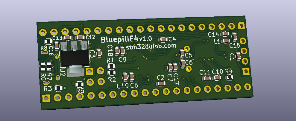
- BluepillF405AP2114.jpg (64.07 KiB) Viewed 248 times
[racemaniac – Mon Oct 16, 2017 7:03 pm] –
I’ve taken a quick go at putting the AP2114 on the board.
I ended up going for the AP2114HA (which is in SOT223 package) first had a look at the sot252 one, but damn is it huge O_O. The 2114HA is a bit smaller (but still WAY bigger than the ap2112 i had), and luckily has GND on its tab (there are 2 versions: the AP2114H & AP2114HA, their pinout differs, and the H has VOUT on its tab).
yeah i always wondered why they do that, always annoyed me that they’re different… then i realised it’s for the trick that you’re using, on 2-layer boards, which i’d never seen before (nice to learn something new) – sandwich between a 3.3v plane on one side and GND on the other. neat. so…. the different types would be for putting on the most suitable side of the PCB. huh. how about that.
And looking at its size, i think it’s big enough, and has a bit ground plane around it to help it cool a bit.BluepillF405AP2114.jpg
size doesn’t matter (hur-hur), it’s the degrees-per-watt figure in the datasheet. you’re looking to do arouuund 250mW @ 3.3v, that’s 8.825 watts. now multiply that by the degrees-per-watt figure for the package…
datasheet:
https://www.diodes.com/assets/Datasheets/AP2114.pdf
there’s two figures for SO-223, one is ambient thermal resistance – 128C/W so we have a figure of 105 degrees that’s on page 7, then another one on page 8 which is 50.9C/Watt (giving a 41.25 degree rise). i don’t know how to interpret these, which one takes precedence, does anyone know?
AP21114HA-3.3TRG1 https://s.taobao.com/search?q=AP2114HA-3.3TRG1 around… RMB 1 which is quite a jump. we’re talking $0.15 instead of $0.05 to $0.07
… still…
[lkcl – Tue Oct 17, 2017 3:17 am] –
size doesn’t matter (hur-hur), it’s the degrees-per-watt figure in the datasheet. you’re looking to do arouuund 250mW @ 3.3v, that’s 8.825 watts. now multiply that by the degrees-per-watt figure for the package…datasheet:
https://www.diodes.com/assets/Datasheets/AP2114.pdfthere’s two figures for SO-223, one is ambient thermal resistance – 128C/W so we have a figure of 105 degrees that’s on page 7, then another one on page 8 which is 50.9C/Watt (giving a 41.25 degree rise). i don’t know how to interpret these, which one takes precedence, does anyone know?
You’re completely messing up your units, calculations and numbers XD
i assume you mean 250mA @ 3.3v. and that would deliver 0.825W to the microcontroller, but would require the regulator to dissipate 0.425W (1.7V voltage drop * 250mA) (assuming 5V input)
So for the ambient resistance that would result in 54.4°C rise
For the thermal resistance to case it would be 21.6°C rise
Since we don’t have that much copper to put against it and dissipate the heat, we’ll probably be in between there, between 30 & 40 degrees or so.
Seems reasonable?
[racemaniac – Tue Oct 17, 2017 6:13 am] –
You’re completely messing up your units, calculations and numbers XD
wark-wark, fail….
i assume you mean 250mA @ 3.3v. and that would deliver 0.825W to the microcontroller, but would require the regulator to dissipate 0.425W (1.7V voltage drop * 250mA) (assuming 5V input)
ohhh…. cool! so… it’s how much power it has to get *rid* of in order to… okaaay i get it.
So for the ambient resistance that would result in 54.4°C rise
For the thermal resistance to case it would be 21.6°C rise
Since we don’t have that much copper to put against it and dissipate the heat, we’ll probably be in between there, between 30 & 40 degrees or so.
Seems reasonable?
yeah i’d say so. 25+40=65C. 60C is tolerable for humans to touch: it’s just outside that… so people won’t get tooo badly burned if they push it to the limit.
[lkcl – Tue Oct 17, 2017 4:14 am] –
AP2112K-3.3trg1 https://s.taobao.com/search?q=ap2112k-3.3trg1 is around RMB 0.36 to 0.50 estimatedAP21114HA-3.3TRG1 https://s.taobao.com/search?q=AP2114HA-3.3TRG1 around… RMB 1 which is quite a jump. we’re talking $0.15 instead of $0.05 to $0.07
How does AMS1117-3.3 compare? Seems to be very commonly used on the cheap modules. Can’t really understand what I am looking at on Taobao…
[bobc – Tue Oct 17, 2017 11:31 am] –[lkcl – Tue Oct 17, 2017 4:14 am] –
AP2112K-3.3trg1 https://s.taobao.com/search?q=ap2112k-3.3trg1 is around RMB 0.36 to 0.50 estimatedAP21114HA-3.3TRG1 https://s.taobao.com/search?q=AP2114HA-3.3TRG1 around… RMB 1 which is quite a jump. we’re talking $0.15 instead of $0.05 to $0.07
How does AMS1117-3.3 compare? Seems to be very commonly used on the cheap modules. Can’t really understand what I am looking at on Taobao…
it’s got a huge voltage drop, so for 5v operation it is ok and very cheap, but for connecting your board directly to a lithium battery, it’s a disaster ![]() …
…
that’s why i ended up going for the AP voltage regulators on my projects. i’m making things i want to connect to a battery, and not first have to boost the voltage to 5V… And there have already been discussions on this forum about this, since others are facing the same problem. That’s why i’d prefer the AP2114, but indeed, quality has its price ^^’
IMHO if you want to run from Lipo, you should use an external power management board which also handles not totally discharging the Lipo
I think you are in danger of over speccing and making the price uncompetative
[RogerClark – Tue Oct 17, 2017 7:35 pm] –
Do both regulators have the same package / footprint?IMHO if you want to run from Lipo, you should use an external power management board which also handles not totally discharging the Lipo
I think you are in danger of over speccing and making the price uncompetative
i usually use batteries with built in protection, so that’s solved on the battery side ![]() . (or with these voltage regulators, you can probably also get away with 3 NiMh batteries, iso 4)
. (or with these voltage regulators, you can probably also get away with 3 NiMh batteries, iso 4)
and the one i chose is not pin compatible with the ams1117… if however we would go for the other one, the AP2114H (with vout on the tab), that one is pin compatible.
but atm, we’re apparantly at about 0.20$ for the regulators, and that’s the only part where we’re going for something fancy, i think that’s bearable? or is it too much?
atm the idea is a cheap & small ap2112 for the analog supply, and the beefier ap2114 for the main supply.
i can try to go for the one that is pin compatible with the cheaper ams1117, but i’ll have to see how i get that to work with the fact that the regulator fits best on the side of the ground plane ^^’
OK.
I’m not trying to go ultra cheap, but from what I’ve seen, the members of the forum are very price sensitive.
I guess we need to have a total BOM cost and work out the percentage of cost for each item, to see if any particular item is substantial part of the overall cost and if so, whether that part can be exchanged for a cheaper alternative
[bobc – Tue Oct 17, 2017 11:31 am] –
How does AMS1117-3.3 compare? Seems to be very commonly used on the cheap modules. Can’t really understand what I am looking at on Taobao…
it’s ebay for china. so.. you know the summary page on ebay? that’s what you’re looking at. so, you apply the same general tricks: ignore anything too low (suspicious), ignore anything too high, and reject any part that has too few sellers. then take the average of the remaining parts, and divide by (appx) 6.5 to get USD.
that way you get a rough idea +/- 20% of how much a part will cost if bought in the markets in shenzhen.
[RogerClark – Tue Oct 17, 2017 11:05 pm] –
@racemanicOK.
I’m not trying to go ultra cheap, but from what I’ve seen, the members of the forum are very price sensitive.
I guess we need to have a total BOM cost and work out the percentage of cost for each item, to see if any particular item is substantial part of the overall cost and if so, whether that part can be exchanged for a cheaper alternative
ok so let’s start that:
- https://s.taobao.com/search?q=STM32f405RGT6 $3 to $4
- https://s.taobao.com/search?q=HC-49USX $0.03 so insignificant
- https://s.taobao.com/search?q=32.768k+mc-306 mc-306 $0.04 or thereabouts: also insignificant
- https://s.taobao.com/search?q=10118194-0001LF USB $0.30
- https://s.taobao.com/search?q=RS-187R05A2-DS-MT-RT reset switch $0.15
then we have either:
- https://s.taobao.com/search?q=AP2112K-3.3TRG1 AP2112K $0.04 or
- https://s.taobao.com/search?q=AP2114HA-3.3TRG1 AP21114HA-3.3TRG1 $0.07
so the processor is by far and above the most significant cost, by a long, long margin. even the SY6280 which would give protected USB-OTG power is only around the $0.07 mark https://s.taobao.com/search?q=SY6280
we’re talking a difference in the BOM of around 1%, absolute maximum 2%, due to the relatively high price of the F405. i also looked up the STM32f411RCT6 but there was too much variation to be able to make an estimate.
the 2114 it is then
can someone summarize the consensus on what to do for usb otg (if there is one)? haven’t had much time to read it all in detail, and tomorrow i’ll probably have some time to work on the board
[racemaniac – Wed Oct 18, 2017 8:07 am] –
thanks for the nice breakdown
the 2114 it is then
can someone summarize the consensus on what to do for usb otg (if there is one)? haven’t had much time to read it all in detail, and tomorrow i’ll probably have some time to work on the board
jumping in (corrections / oversight appreciated) i think using a MOSFET-gated-to-ground (just as in the Due schematic) and the SY6280 for enable/disableable power-protection will give you OTG power control with the minimum component count. you’ll have to jump back a few pages to find the schematic images i posted (gaahhh i really don’t like this aspect of forums – roger, we need that wiki page, man!)
this one: http://stm32duino.com/viewtopic.php?f=1 … 140#p35772
also the USB ID line is only checked at plug-in time and for USB2-only-client devices it’s not even relevant. so i think you’re good to go, just don’t put any extra components on it (no resistors, no capacitors, nothing) then it can double up as one of the UART lines.
The hazard I see is that if a cable is plugged into the pill, it could have the ID connected to ground. If you set that GPIO to output 1, it will be sinking straight to ground and will likely burn out. Therefore I suggest all that is needed is a current limiting resistor, e.g. 10k, to allow the GPIO port to be shared.
[bobc – Wed Oct 18, 2017 11:22 am] –
There seems to be some confusion about the ID pin and how it is used. The purpose of the ID pin to identify a “host” when two *devices* are connected together. The ID pin is grounded at one end inside the cable, the ID pin is never driven by the CPU. A PC is always a host, the USB A connector does not have an ID pin.The hazard I see is that if a cable is plugged into the pill, it could have the ID connected to ground. If you set that GPIO to output 1, it will be sinking straight to ground and will likely burn out. Therefore I suggest all that is needed is a current limiting resistor, e.g. 10k, to allow the GPIO port to be shared.
the reference design in the appendix doesn’t have any such resistor.
the datasheet DocID022152 page 115 section 5.3.6 table 48 shows that PA10 and PB12 have a 10k pull-up and 10k pull-down resistor on-board the IC.
if we suggest that there should be 10k resistors on the ID pin, then by the same logic *all* pins should have 10k resistors on them… because all pins could be used as outputs and “accidentally grounded”.
so, this case should be covered in the instructions: a large warning “do not switch the ID pin to an output and then also plug in a USB OTG device”.
honestly i feel that once you start treating people as unable to read instructions, it never ends. 20 years ago i knew someone who worked for SCO (before they went bad). he taught me a lovely quote: “if you make something idiot-proof, only idiots will use it”.
put a resistor in series and then you can never use that pin for anything other than purposes for which a 10k resistor happens not to interfere.
[racemaniac – Wed Oct 18, 2017 11:52 am] –
Can someone maybe draw me a schema on how we now want to hook it up? i’m getting lost ^^’
again: look at the diagrams i sent in the link to the earlier discussion. here is the link again. diagram 3 in this link http://stm32duino.com/viewtopic.php?f=1 … 140#p35772
that diagram is straight out of the appendix in the datasheet. page 187, figure 95, document ID DocID022152 Rev 8, filename en.DM00037051.
[lkcl – Wed Oct 18, 2017 12:05 pm] –[racemaniac – Wed Oct 18, 2017 11:52 am] –
Can someone maybe draw me a schema on how we now want to hook it up? i’m getting lost ^^’again: look at the diagrams i sent in the link to the earlier discussion. here is the link again. diagram 3 in this link http://stm32duino.com/viewtopic.php?f=1 … 140#p35772
that diagram is straight out of the appendix in the datasheet. page 187, figure 95, document ID DocID022152 Rev 8, filename en.DM00037051.
that diagram isn’t quite clear to me, what is the current limiter switch? (is that the SY6280?), and so i’ll have to use an extra pin for this voltage switch (one that is not part of the usb pins of the f4?)
concerning the resistor on ID pin: if i put the resistor between the pad & the usb port (and not between the f4 and the pad), we have best of both worlds ![]() . no shorts when doing something wrong, and the pad not having the resistor messing with it
. no shorts when doing something wrong, and the pad not having the resistor messing with it ![]() .
.
[racemaniac – Wed Oct 18, 2017 12:50 pm] –[lkcl – Wed Oct 18, 2017 12:05 pm] –[racemaniac – Wed Oct 18, 2017 11:52 am] –
Can someone maybe draw me a schema on how we now want to hook it up? i’m getting lost ^^’again: look at the diagrams i sent in the link to the earlier discussion. here is the link again. diagram 3 in this link http://stm32duino.com/viewtopic.php?f=1 … 140#p35772
that diagram is straight out of the appendix in the datasheet. page 187, figure 95, document ID DocID022152 Rev 8, filename en.DM00037051.
that diagram isn’t quite clear to me,
you wire up the USB and ID direct. no resistors.
what is the current limiter switch? (is that the SY6280?),
yyup. and the 5V regulator thingy is just the MOSFET-that-has-the-gate-tied-to-GND. it’s being used, in effect, as a diode, stopping power getting back up the line. the absolute last thing you want is a current bun-fight between two 5V supplies.
you could just use a schottky diode instead but if you do try to find one with the absolute lowest possible voltage drop. the MOSFET’s probably being used (effectively) as a diode because its voltage drop is (i presume) very low?
and so i’ll have to use an extra pin for this voltage switch (one that is not part of the usb pins of the f4?)
yyup.
concerning the resistor on ID pin: if i put the resistor between the pad & the usb port (and not between the f4 and the pad), we have best of both worlds ![]() . no shorts when doing something wrong, and the pad not having the resistor messing with it
. no shorts when doing something wrong, and the pad not having the resistor messing with it ![]() .
.
i don’t think it’s a good idea to do anything other than follow the reference design. i do not think it is a good idea to assume that the users need to be… molly-coddled is a good word to use.
i repeat: if you expect that people will damage one particular output and are going to “protect” it with a 10k resistor, you MUST now put a 10k resistor on EVERY single pin…. just in case they quotes might damage the board quotes. this is treating users like idiots, because it’s making the board “idiot-proof”. don’t do it. if they ignore the instructions and blow up the processor, they can buy another board and not make the same mistake again.
again, i repeat: you don’t know the consequences on people’s designs of forcing them to have a 10k resistor in series with that pin. some shields may simply… fail to work properly because the supplied current is insufficient to drive the 10k resistor high/low/whatever. if they use it as an analog output (PWM-driven) you could end up *changing* the output compared to the original BluePill because there’s an extra 10k resistor in the circuit that the shield didn’t anticipate being there, which alters the RC circuit in unpredictable ways.
don’t do it.
so ignoring the CARD_VCC 10k pullup, you can see they’ve put a 1k in series with the USB_ID line. that’s *between the F4 and the USB connector* *NOT* repeat *NOT* between the pinheader and the F4.
i’ll try to find some other schematics just to make absolutely sure.
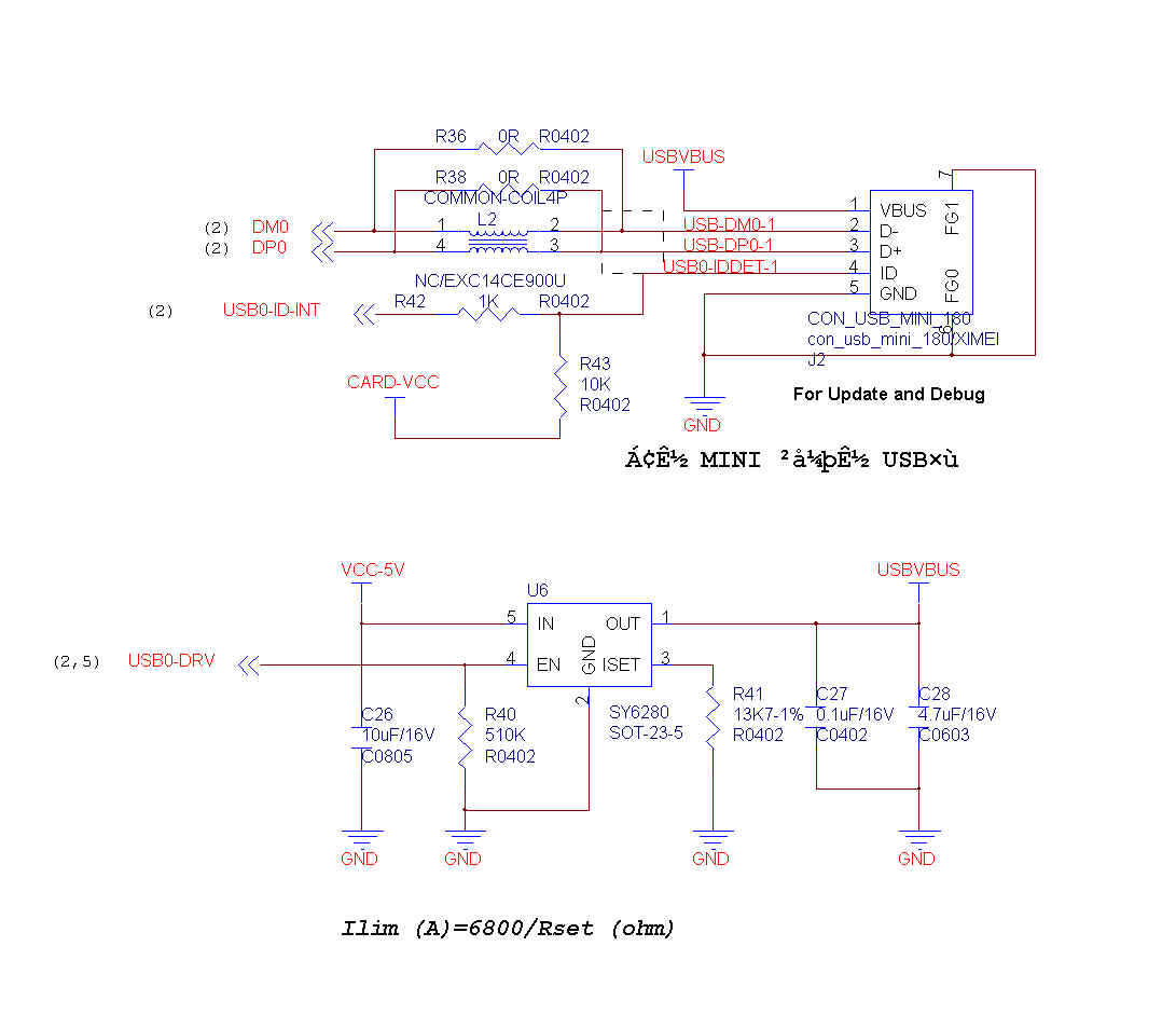
- Untitled1.jpg (60.19 KiB) Viewed 187 times
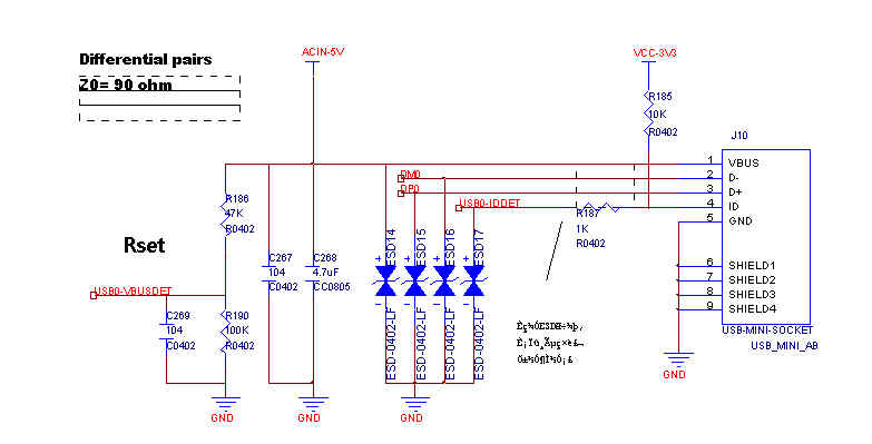
- Untitled1.jpg (28.61 KiB) Viewed 187 times
[lkcl – Wed Oct 18, 2017 1:18 pm] –
again, i repeat: you don’t know the consequences on people’s designs of forcing them to have a 10k resistor in series with that pin. some shields may simply… fail to work properly because the supplied current is insufficient to drive the 10k resistor high/low/whatever. if they use it as an analog output (PWM-driven) you could end up *changing* the output compared to the original BluePill because there’s an extra 10k resistor in the circuit that the shield didn’t anticipate being there, which alters the RC circuit in unpredictable ways.don’t do it.
Sorry, your argumentative style is simply illogical and idiotic. I made a simple and practical suggestion and you’ve gone into some sort of mental meltdown. Clearly, a non-idiot can simply remove the resistor if they don’t need it, but even a non-idiot will find it harder to replace the CPU if they burn out a pin.
I’m out – good luck.
Something like (where the dashes is the electrical connection):
USB ID PIN——1k——header_pin——MCU PIN.
If nothing is connected in the USB connector (so USB ID PIN is floating), then the 1k is not going anywhere, and should not cause any trouble.
If the Datasheet calls for it, it should be used. If it doesn’t call for it, but can be used without affecting anything, I would think is better to use it (if the pin is in a header so a user may decide to use it for something else). It’s not about protecting every single pin, but just 1 pin that has a higher risk of being shorted to ground.
If that pin is not routed to any header, only to the OTG USB ID pin, the I think we should just go with what the datasheet calls for and not think on it anymore. There is no point protecting the pin if it’s not available in a header to be used as GPIO.
[bobc – Wed Oct 18, 2017 3:43 pm] –[lkcl – Wed Oct 18, 2017 1:18 pm] –
again, i repeat: you don’t know the consequences on people’s designs of forcing them to have a 10k resistor in series with that pin. some shields may simply… fail to work properly because the supplied current is insufficient to drive the 10k resistor high/low/whatever. if they use it as an analog output (PWM-driven) you could end up *changing* the output compared to the original BluePill because there’s an extra 10k resistor in the circuit that the shield didn’t anticipate being there, which alters the RC circuit in unpredictable ways.don’t do it.
Sorry, your argumentative style is simply illogical and idiotic. I made a simple and practical suggestion and you’ve gone into some sort of mental meltdown. Clearly, a non-idiot can simply remove the resistor if they don’t need it, but even a non-idiot will find it harder to replace the CPU if they burn out a pin.
I’m out – good luck.
he’s indeed having a bit too much of a meltdown ^^’
but don’t leave the discussion, any feedback is useful, let’s not get discouraged because of this ![]()
[bobc – Wed Oct 18, 2017 3:43 pm] –
Sorry, your argumentative style is simply illogical and idiotic. I made a simple and practical suggestion and you’ve gone into some sort of mental meltdown. Clearly, a non-idiot can simply remove the resistor if they don’t need it, but even a non-idiot will find it harder to replace the CPU if they burn out a pin.I’m out – good luck.
ok, your choice. i’ll assuming you won’t be reading this thread any more. very strange, because he should have seen the follow-up messages which indicated that i realised i’d made a mistake, and double-checked with some other schematics that i have here which show that adding in a series resistor is quite common.
so, would it be reasonable to assume that the users of this board would be happy to remove an 0402 component from a board? what if they want to put it back on again, later? so no – i wouldn’t have thought so. i know from experience that 0402 components are exceptionally hard to hand-solder, if you want to put them back on, and even taking them off in the first place risks damaging or losing them: they tend to stick to the soldering iron tip and need to be removed very very quickly with tweezers.
so, the logic behind not putting the resistor in series between the F4 and the header stands: it changes the characteristics of the pin, such that existing shields with which this board – deliberately named the BluePillF4 and deliberately made to be pin-compatible so as to save people on the cost of having develop or buy yet another set of incompatible shields – may fail to work.
i don’t see anything illogical or idiotic about that: if there is i have no problem with people saying so (publicly).
[victor_pv – Wed Oct 18, 2017 3:59 pm] –
Regarding the 1k resistor, if it’s planned between the USB ID pin and the header pad, then it would not affect if the user doesn’t use USB on the go.
Something like (where the dashes is the electrical connection):
USB ID PIN——1k——header_pin——MCU PIN.
yehyeh, that’s it: that would do it. i didn’t quite understand what racemaster was referring to initially: your ascii art makes it clear that we’re talking about the same thing.
If that pin is not routed to any header, only to the OTG USB ID pin, the I think we should just go with what the datasheet calls for and not think on it anymore. There is no point protecting the pin if it’s not available in a header to be used as GPIO.
http://wiki.stm32duino.com/index.php?title=Blue_Pill pinout’s towards the bottom.
i did the analysis a couple days ago: for pin-compatibility / interoperability with pre-existing bluepill shields there is no other option but to use this particular pin as GPIO.
right at the beginning of the thread (somewhere on page 3 or 4) i asked roger if pin-compatibility was strictly necessary: he said it was because there is a huge range of pre-existing bluepill shields and it would be pain (costly) to force people to make more to yet another non-interoperable shield standard.
[racemaniac – Thu Oct 19, 2017 3:28 pm] –
@22R & 1k5 resistors: not sure for the 22r, but i see something like that used in most cases, the 1k5 is not needed for the F4, but if we leave it in, the board is also compatible with an F1 which does need it
ok – so NC for F4. note recorded to that effect in schematic page?
@mosfet: the one i chose is slightly worse in specs (bit higher on resistance), but also a bit smaller, all in all very very similar ![]() .
.
nice.
@sy6280 resistor, the formula is A=6800/Rset (ohm) . so for 0.5A it’s 13.6K ![]() . i thought a bit extra would be nice, but i’ve seen schematics going for a value close to 13.6k
. i thought a bit extra would be nice, but i’ve seen schematics going for a value close to 13.6k
doh! ![]()
@divider bridge: do i bring it to for example PC8, or to the dedicated pin for it on the stm32f4 (PA9). It will then basically result in a weak pullup on the TX of the serial line we wish to not compromise, not sure how well u(s)art can cope with that.
otherwise i can do it to pc8 and then we have to manage it ourselves, not have the peripheral do it for us. (or do it via a jumper… but we’re already running short on space >_<)
yeah i didn’t realise in the reference / appendix they just have PA9 wired directly to VBUS. if that’s what they’re doing then… it *should* be listed as a 5v-tolerant pin…. that means looking up table 6 (page 46…) “FT” means “five tolerant”… aand yes, age 55 PA9 is 5v-tolerant.
ok so it’s fine. direct-wired, no resistor-divider bridge. PA9 can be used as OTG_FS_VBUS detect.
Or a Wiki page, Roger? We are up to 20 pages for this thread, and it is getting tedious to find a piece of information!
Putting the files in github would be the best solution
I can put the latest version from @racemaniac in that repo, but he has not posted updates files for several days
Please provide PDFs/GIFs along with CAD files, so that one can see the result on mobile devices without Kicad…
the schema is already updated with the extra USB things, but the pcb isn’t (and the connection between vbus an PA9 hasn’t been made yet in the schema).
the new parts haven’t been annotated yet/footprint selected (the selected mosfet is sot223)
- BluepillF4v1.0e.zip
- (215.72 KiB) Downloaded 15 times
In case its easier for people to manage this via github, I’ve added @racemaniacs board to my existing github repo
https://github.com/rogerclarkmelbourne/ … ill_Boards
I removed my abandoned attempts, and I’ve renamed the KiCad version of the STM32Stamp board, back to its original name.
May be one day… a F405 or something like that… I could give it a try… why not…
Here are the Schematics and PCB files in PDF.
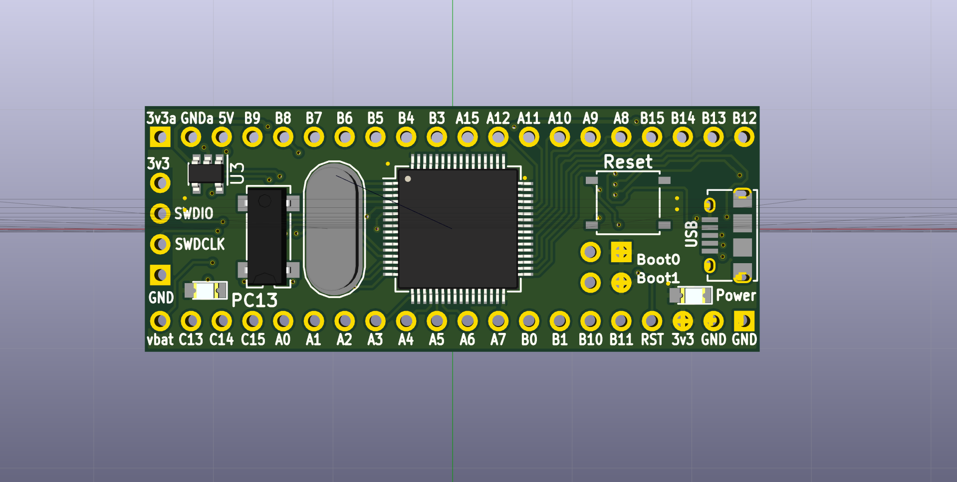
- BluepillF4_3D_Top.png (188.53 KiB) Viewed 147 times
I’ll add those files to the repo
Edit.
Those files should now be in the repo
I just put them in the root of the repo.
PS. I think we need a BOM CSV file so that we can calculate the price etc
No point doing gerbers yet, as the design is not stable
Whats the best way to resolve this when I open the schematic ??
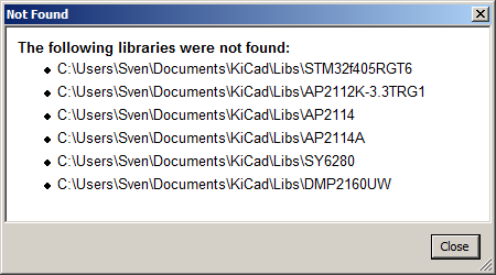
- missing_libs.png (6.74 KiB) Viewed 143 times
https://3dwarehouse.sketchup.com/model/ … -Lead-Free
I noticed on the Teensy 3.6 that it has SMD pads on the bottom, because the MCU has more GPIOs etc than there are though holes on the PCB
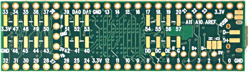
Looking at the PCB layout, there may be scope to do the same thing for some of the unused pins
[Squonk42 – Thu Oct 19, 2017 10:22 pm] –
Yes, but this is just bending the pins for through-hole, the main body should be OK.
OK
I tried to download that file, but there is a whole load of license conditions which I’m not sure may preclude us from adding it to an open source project
It may not look so pretty, but its probably easier to knock up something in OpenSCAD
[RogerClark – Thu Oct 19, 2017 10:25 pm] –[Squonk42 – Thu Oct 19, 2017 10:22 pm] –
Yes, but this is just bending the pins for through-hole, the main body should be OK.OK
I tried to download that file, but there is a whole load of license conditions which I’m not sure may preclude us from adding it to an open source project
It may not look so pretty, but its probably easier to knock up something in OpenSCAD
As it is my own work, I will send you this 3D model under a compatible licence of your choice, let me know the more appropriate.
I wall’have to figure out how to convert it to a format that Kicad can read using free tools like Blender or Openscad
Do you know which formats are supported by Kicad?
don’t make it too complicated for me when i’m back on monday :p
It seems that KiCad does not support all types of VRML but that the version exported by FreeCAD works OK.
Also Wings3D can export in the correct type of VRML
But as I was creating my models in OpenSCAD, the best way I found was to open the SCAD file in FreeCAD, then export to WRL
(Note. FreeCAD seems to have 2 copies of the SCAD object when it imports, so I had to select the second “group” e.g. “group11” before I could export.)
I downloaded that model and imported the DAE file into FreeCAD, then selected all the objects and exported as WRL, and loaded that into KiCAD, but it seems to not have any colour information, so it was all the same colour as the PCB (green) ![]()
The scale was also quite different, and I had to set it to 0.005 to be roughly correct. But this seems a very strange scale factor e.g. I could understand if it was 0.001 for mm instead of metres, or perhaps 0.0025 for mm to inches etc (or perhaps the reciprocal of that value)
But 0.005 seems strange.
I am not an expert in FreeCAD, I only used it to export from OpenSCAD to VRML, for KiCad and it seemed to retain the colours defined in OpenSCAD, but this doesnt seem to apply to Collada format.
FreeCAD does not seem to support importing Sketchup files ![]()
To set the colours you could use Wings3D but its a pain to have to select each object in the model and set its colour
What format was the model originally created in ? Sketchup ?
[RogerClark – Thu Oct 19, 2017 7:52 pm] –
I am. not sure a wiki page would help
from experience of 20+ years collaborating in public i know that it helps enormously… but only if there’s someone actually prepared and motivated to use and maintain it… which because of seeing how amazingly effective they are, year after year, project after project, i most certainly am.
for example: when doing the reverse-engineering of the HTC BlueAngel and other smartphones, we used the wiki to house notes, discussions and so on.
already i’ve been forced into repeatedly giving people back-links to schematic diagrams… which i cannot even find myself and am forced to click, click, click, page back, page back.
those diagrams should *be on the wiki*, where i would bookmark it as a pinned tab, and would reasonably expect people to have it open as well, next to the tab for this [throw-away-style, completely impossible-to-find-anything except the most absolute and immediate latest replies] discussion.
forums are great for communicating in an immediate fashion but for actual information, which people clearly can’t be expected to keep in their heads, they’re worse than useless.
a wiki – which is a STATIC real-time editable document – makes up for that.
Putting the files in github would be the best solution
… which as an ethical software libre advocate i can’t contribute to. for reasons why, see https://directory.fsf.org/wiki/Collecti … placements and https://www.gnu.org/philosophy/who-does … ve.en.html
also: putting the *source* code online is not what is primarily needed here. we need *discussion* documents, research links, links to the datasheets, links to schematic reference diagrams and so on.
yes sure github has a wiki feature… but i cannot use it. so i will be forced into typing out “can someone please put this on the wiki”, “can someone please upload this image to the wiki”, “can someone please put this research link on the wiki” and after about the fourth time people will get really tired of that and will stop replying.
… been at this a long time, roger ![]()
It looks like the Collada format is loosing color information.
Anyway, there isn’t much color in it: the body is a kind of mate greyish tin metal, there is a black plastic inner body with gold contacts + SMD pins.
or will i keep doing all the changes to the pcb?
[racemaniac – Fri Oct 20, 2017 9:18 am] –
what i am wondering though is on github or so how we’ll handle the pcb project, unlike code it’s something that doesn’t lend itself to easy merging ^^’
or will i keep doing all the changes to the pcb?
Only put it in github so people could access the latest version from the same place all the time.
To save people having to scroll backwards from the last post, to the last time you attached a zip
I don’t know of a way to do co-operative development of PCB’s or Schematics
[RogerClark – Thu Oct 19, 2017 10:15 pm] –
Missing libs ??
Same here…
[lkcl – Thu Oct 19, 2017 2:56 pm] –
they use a FDN340P if that helps
Nice, but FDN304P is better
[racemaniac – Thu Oct 19, 2017 3:28 pm] –
@mosfet: the one i chose is slightly worse in specs (bit higher on resistance), but also a bit smaller
And where to buy??
2y ago I ordered a couple of IRLML6402, they do work outstanding for me, cheap and widely available.
Last year I got another tip: DMP1045U, harder to find but maybe one of the best possibilities ATM.
Why, the hell, did you change the microUBB printout?
I’ve lying a couple around here, no one matches your new one ![]() (
(
[RogerClark – Fri Oct 20, 2017 9:58 am] –[racemaniac – Fri Oct 20, 2017 9:18 am] –
what i am wondering though is on github or so how we’ll handle the pcb project, unlike code it’s something that doesn’t lend itself to easy merging ^^’
or will i keep doing all the changes to the pcb?Only put it in github so people could access the latest version from the same place all the time.
To save people having to scroll backwards from the last post, to the last time you attached a zip
which helps with schematics and PCB files… but does nothing to help with the research of parts, research, publication and discussion of reference designs and so on. for all of that we are still forced to repeatedly cross-reference back to older posts. forum software is a total failure when it comes to collaborative development, roger. it’s perfect for simple real-time (unimportant) discussions. the most extreme case i ever heard was a reference telling people to look for a schematic on page *746* of a 1,000-page discussion.
I don’t know of a way to do co-operative development of PCB’s or Schematics
there was one project i heard of which was an online PCB editor, in theory it would be possible to contribute/collaborate.
kicad helps inasmuch as you can split schematics into multiple pages and use git pull to merge them in. i spoke to the developers a long time ago and got them to remove the ridiculous practice of putting (and modifying) timestamps into the text output every time you hit “save”. it was massively interfering with collaborative development.
PCBs… no. you just have to manually hand off to another person, ask them to do mods, and refrain from editing until they’re finished. in theory, as kicad is a text-based file format you could merge changes but i wouldn’t want to try it.
[bianchifan – Fri Oct 20, 2017 11:12 am] –[RogerClark – Thu Oct 19, 2017 10:15 pm] –
Missing libs ??Same here…
[lkcl – Thu Oct 19, 2017 2:56 pm] –
they use a FDN340P if that helpsNice, but FDN304P is better
[racemaniac – Thu Oct 19, 2017 3:28 pm] –
@mosfet: the one i chose is slightly worse in specs (bit higher on resistance), but also a bit smallerAnd where to buy??
2y ago I ordered a couple of IRLML6402, they do work outstanding for me, cheap and widely available.
Last year I got another tip: DMP1045U, harder to find but maybe one of the best possibilities ATM.Why, the hell, did you change the microUBB printout?
I’ve lying a couple around here, no one matches your new one
the point was to have a micro usb socket that could be easily sourced, so they went for that one, but indeed, i can’t find it on aliexpress either, so that part also annoys me a bit ^^’
but i do understand that as it currently is, it’ll be easier to have actually produced by someone.
However, this socket takes up a bit more space than the one i used originally, so once we’re done, i can make a second version of the files with parts easily found on aliexpress/ebay, and those can be used for people who want to make their own boards ![]()
and now i’m really leaving for the weekend, see y’all on monday ![]()
Look at this one, only 0.06 RMB:
https://item.taobao.com/item.htm?id=531741597795
EDIT: It is a clone of this Molex connector:
http://www.molex.com/pdm_docs/sd/476420001_sd.pdf
You can find the 3D model here:
http://www.molex.com/molex/products/dat … ECTORS.xml
[Squonk42 – Fri Oct 20, 2017 1:47 pm] –
A mid-mount micro USB socket like the one used in the Bluepill would be the best, it makes the overall board thinner and it has 4 large TH legs that prevent tearing it apart from PCB when plugging/unplugging the cable.Look at this one, only 0.06 RMB:
https://item.taobao.com/item.htm?id=531741597795EDIT: It is a clone of this Molex connector:
http://www.molex.com/pdm_docs/sd/476420001_sd.pdfYou can find the 3D model here:
http://www.molex.com/molex/products/dat … ECTORS.xml
excellent – it’s really important to find datasheets / part numbers for all components… *and* also then check that there’s dozens of suppliers with that exact part on taobao. you can’t do it the other way round (or… it’s hell to try): the market vendors don’t care about datasheets.. or if they do they have them on internet-disconnected personal laptops, no website, and the best you can do to contact them is email them, call them or use QQ. all of which requires that you speak mandarin.
so… good find, sqonk42, that’s saved a lot of hassle, finding the molex part number.
[edit] – just as a safety check i took most of the chinese characters, the 5P etc. etc. and dropped them into a search: it came up with 2 pages of vendors selling parts that look exactly like this one, which isn’t quite enough to be “safe” that they’re not all rip-off merchants. however as it’s a molex clone it’s probably okay.why?
well… in 2 days time when racemaster comes back, there will be about… 2 or 3 more pages of discussion. he won’t see any of that… so what we will be forced to do is: *remember* that the part is there, and do page-back, page-back, page-back, scroll, scroll, scroll… and eventually, if we’re really lucky, not miss it, and be able to refer him to it.
however… if there was a wiki, which he’d bookmarked, we could just say “go look at the wiki reference section we added an excellent USB mid-mount connector”
wiki pages are *really important*. i would set one up however im doing so it makes my personal web server resources a permanent part of the stm32duino infrastructure, which i don’t feel is appropriate for me to do.
[lkcl – Fri Oct 20, 2017 4:03 pm] –
[edit] – just as a safety check i took most of the chinese characters, the 5P etc. etc. and dropped them into a search: it came up with 2 pages of vendors selling parts that look exactly like this one, which isn’t quite enough to be “safe” that they’re not all rip-off merchants. however as it’s a molex clone it’s probably okay.
Yes, here is the corresponding query:
https://s.taobao.com/search?q=USB+5PIN% … =price-asc
According to Google, “USB 5PIN沉板 MICRO 5P MK5P 沉板 0.8mm母座 四脚插 USB插座” translates into “USB 5PIN sink board MICRO 5P MK5P sink board 0.8mm female four feet plug USB socket”, where “sink board” probably means “mid-mount” and “four feet plug” means “4 Through Hole Solder Tabs”.
2D drawing and 3D STEP files here:
http://www.alps.com/prod/info/E/HTML/Ta … CE010.html
It can be found for 0.10 RMB on TaoBao from many vendors:
https://s.taobao.com/search?q=SKSGACE01 … =price-asc
It could be interesting too to replace the tall and bulky BOOT header & jumpers by an additional similar button for BOOT0, much like the dual-button solution used on NodeMCU boards for RESET/FLASH (page 6):
https://github.com/nodemcu/nodemcu-devk … T_V1.0.PDF
[Squonk42 – Fri Oct 20, 2017 9:17 pm] –
Regarding the reset button switch: I used the ultra-small (3.5 mm L x 2.7 mm W x 1.4 mm H) ALPS SKSGACE010 in some of my existing designs:
2D drawing and 3D STEP files here:
http://www.alps.com/prod/info/E/HTML/Ta … CE010.htmlIt can be found for 0.10 RMB on TaoBao from many vendors:
https://s.taobao.com/search?q=SKSGACE01 … =price-ascIt could be interesting too to replace the tall and bulky BOOT header & jumpers by an additional similar button for BOOT0, much like the dual-button solution used on NodeMCU boards for RESET/FLASH (page 6):
https://github.com/nodemcu/nodemcu-devk … T_V1.0.PDF
Just a thought, but if Boot0 was a button, perhaps we could also run a track to an unused GPIO pin, so in normal operation it doubled as a USER button.
(though potentially glitches on the GPIO pin at boot time could cause problems
[RogerClark – Fri Oct 20, 2017 10:33 pm] – Just a thought, but if Boot0 was a button, perhaps we could also run a track to an unused GPIO pin, so in normal operation it doubled as a USER button.
(though potentially glitches on the GPIO pin at boot time could cause problems
IIRC, this was the option used in the Maple Mini, where the BOOT0 switch was also connected to PB8:
https://github.com/leaflabs/maplemini/b … lemini.pdf
I forgot that…
[RogerClark – Sat Oct 21, 2017 8:01 pm] –
Thanks…I forgot that…
Yes, but this means that it was a good idea ![]()
So we may keep it!
Another subject, MicroSD, which is a superior feature of the F405: look at this beauty:
http://www.molex.com/molex/products/dat … SOCKET.xml
… Only 11.95 mm wide, meaning that it fits between the BP rows of pins… May be worth to provide the footprint on PCB bottom side (at least if there is still space), although they are not even expensive on TaoBao:
https://s.taobao.com/search?q=104031&ty … =price-asc
Roger, can you do that and bookmark posts like the one with the usb part in the first post? that’s easy and effective, without consuming much time.
I’m not sure what yoi mean by Bookmark..
Re:wiki
Its a refernce not a dev space
threads titled for the component ?
stephen
[victor_pv – Sat Oct 21, 2017 8:39 pm] –
Guys, without creating any wiki, is really easy for the OP to modify the first post and add links to the relevant posts in the thread.Roger, can you do that and bookmark posts like the one with the usb part in the first post? that’s easy and effective, without consuming much time.
that places the burden of maintaining the references onto the OP (in this case, roger). do you think he would be ok to make 4 to 5 edits per week, as everyone asks him, “please can you update the 1st post to put this research on it? please can you put this on the 1st post roger? please can you upload this image onto the 1st post roger?” how long do you think he would tolerate doing that, and do you feel that it’s acceptable to flood an *ALREADY* overloaded forum with 1980s-style AOL “metoo” postings?
also: will roger be up at the same time that i am? i am on GMT+7 (Taiwan), i presume that there are also people in the US and also EU timezones.
the point of a wiki page is that it is collaborative: no one person becomes a critical bottleneck.
[zmemw16 – Sun Oct 22, 2017 1:05 am] –
i wonder maybe if it’s time for a hardware-snippets category ?
threads titled for the component ?stephen
let’s think that through. how could several people contribute to – edit – posts within that hardware-snippets category? they can’t, can they? not unless the username and password of the account used to make the posts is published – publicly – and i doubt very much whether that would be acceptable.
so what would happen would be that anyone spotting a mistake or wishing to contribute a similar circuit would be forced to post underneath. if the OP is no longer a member of the forum, the information becomes out-of-date, or extremely fragmented.
bottom line: *there is no substitute for a wiki*. forums have an extremely good purpose, but they cause people to lose critical information. wikis are good at recording and researching “static” information, but they are absolutely useless for having lengthy and detailed conversations.
the COMBINATION of the two is what makes a successful collaborative project.
[RogerClark – Sat Oct 21, 2017 8:54 pm] –
Re:wikiIts a refernce not a dev space
ah, you mean: you want to maintain the stm32duino wiki *as* a static reference, maintained, controlled and reviewed only by a few people to provide specific information? that’s a good resource to have.
unfortunately, though, as you can see from this current discussion, where people are extremely heavily inconvenienced by not being able to record *active* research, having to constantly refer to back-links time and time again, the forum alone is not enough, and neither is a (restricted, static, edited-after-the-fact wiki, no matter how good that resource genuinely is)
this is an example of how, back in 2003, we used a wiki (and irc) to collaborate and communicate over 3 different timezones:
https://forum.xda-developers.com/wiki/H … l/Research
that one we organised very well, splitting it into different pages.
a page where we took a different approach (single-page) is here:
https://forum.xda-developers.com/wiki/H … l/Research
basically we used it to record all of the pictures *as we were going along*. someone would publish and upload a photo of the PCB, then someone else would do the research to find datasheets.
can you see how incredibly useful that would be to have here?
can you see how staggeringly-less hassle it would be to no longer force everybody to rummage through 24 (and increasing) pages to find the exact same information?
it’s really hard to be discussing multiple things like this >_<.
[victor_pv – Sun Oct 22, 2017 2:07 pm] –
Roger perhaps a new section in the Wiki for this board, which hopefully will be a reality soon and need a page in the wiki anyway, could have that “research” section?
ok, so just so you know, people, it’s potentially quite a lot of extra administrative / sysadmin work for roger: the wiki’s not set up to permit new logins, so that just slams spammers out cold. very simple, very effective. allowing people accounts that need approval doesn’t shut out spammers: it just… adds to the administrative burden for roger as the spammers will just keep trying anyway. allowing people to have arbitrary accounts (without a sysadmin check) means it risks automated spam-attacks / automated spam-editing. they’re not even personal: regular internet port-scanning takes place by the mafia (in several countries), etc. etc. and as it’s wikimedia the attack scripts literally roll out automatically. this is why i use non-popular web software such as ikiwiki.
the advantage however would be a huge reduction in stress levels of everyone on the forum, as well as an administrative reduction in the development of the “static” reference information (added post-fact) as the “research” material *actually morphs into* reference information (as you can see from those xda-developers examples i worked on over a decade ago), completely saving you (roger) the job of doing it entirely by yourself without any assistance.
then a few people in this thread discussing it would need to register, but it’s now the same when entering this forum. Roger will have to add a few accounts to the wiki, and we’ll be started.
[racemaniac – Tue Oct 24, 2017 7:49 am] –
can’t we discuss it on the wiki, and only allow logins the way it is now?
interesting suggestion… from experience i’ve seen repeated evidence that complex discussions quickly become absolute hell-on-earth for different reasons when using a wiki as a “discussion forum”. each type of online collaborative tool has different strengths and weaknesses.
wikis are great for developing and researching information, that, once finished becomes the “reference guide”, but you try and actually maintain a conversation? you can’t find *anything* because it’s all jammed into one non-linear page, where people are perfectly allowed to just… arbitrarily insert responses anywhere into the document. even if everybody follows the “rules”, after even a few hours absolutely nobody can find anything.
forums are great for having linear conversations online, as if people were in the same physical room, but spread out over time. there’s even a way to “catch up” on the discussion by going back a few messages, you can embed images and so on and there’s no special software needed. but if you actually want to develop something complex, absolutely nobody but the world’s geniuses can hold that much information in their heads, and using the forum *alone* everyone feels like they’re desperately treading water on a ladder that’s constantly sinking into the depths of the ocean, drowning them in messages and information.
mailing lists – particularly with archives – are a great way to do the same job as forums except that they have the advantage of contributors being able to go “offline” at their own discretion. many highly technical collaborators still do this, and they take in vast quantities of messages per day and can keep up-to-date very very quickly with literally dozens of simultaneous conversations across a huge number of lists. however it requires quite strict communications discipline (outlined in “mailing list netiquette” documents) that… most forum users are incapable of understanding, respecting or following… to the detriment of absolutely every technical contributor on that list. so the admin sometimes has to get quite strict about enforcing the netiquette.
irc is great for keeping people in touch in real-time, the problem being they actually have to be *in* real-time i.e. on the same time-zone. when working with xda-developers community members, we found that with the addition of a “bot” that logs everything and publishes it online every 24 hrs (just in case our individual internet connectivity went down) we could leave IRC running 24×7 (or in case of a disconnection refer back to the bot logs) and thus actually have a conversation spread out over 36-72 hours. but if we had tried that *without* the wiki to record detailed notes it would have been a total nightmare.
anyway: it really is down to you, roger, also what you feel comfortable with setting up (and maintaining) i have the ability to set up online resources (i run my own server) but as i mentioned before, it would not be appropriate for me to set up “unofficial” wikis / other online document collaboration tools for users of this forum to use, as they would quickly become part of the infrastructure here: the very first URL/link posted and that’s it, it’s no longer “unofficial”. why? well, if i decide i needed the space on my server the records would be… lost, and any references / archive links here in this forum would be terminated as dead-ends. that would be… bad ![]()
and for the discussions, the thread is becoming a bit hard. we’re discussing usb, extra pads for the pins, the usb connectors, the voltage regulators all at the same time >_<
it’s becoming a bit much for 1 thread (imo)
lessons learnt ?
srp
[zmemw16 – Tue Oct 24, 2017 8:26 pm] –
isn’t this about how this forum was started, when it was originally created from an excessively large thread ?
lessons learnt ?
srp
XD
indeed XD
a (temporary) forum subsection so we could split this up in several threads would also work ![]()
it’s a nice to have, but not sure if it’s worth it since pcb area is already short in supply as it is ^^’
(and even more so if we want to offer smd pads for the pins currently not broken out)
[racemaniac – Tue Oct 24, 2017 7:41 pm] –
not sure if you know there already is a wiki: http://wiki.stm32duino.com
roger has locked it so that nobody can create an account. only authorised people who already have login details are permitted to edit pages.
[racemaniac – Wed Oct 25, 2017 8:40 am] –
concerning the usb connector: i know of the mid mounted ones, but is the board being a tiny bit thinner that much of an advantage? it also takes away space to route the usb traces/place its resistors, and a usb micro connector is already pretty thin.
it’s a nice to have, but not sure if it’s worth it since pcb area is already short in supply as it is ^^’
(and even more so if we want to offer smd pads for the pins currently not broken out)
Not only thinner, but stronger: the micro USB connectors are supposed to withstand more plug/unplug cycles than mini USB ones, which in turns support more cycles than the original USB type B (the square, bulky one). However, being SMD with tiny dimensions make them very easy to break away with some traces from the PCB if you are too rude or don’t pull/push straight.
This was a major cause of failure on early Red/Blue Pill boards with such micro USB SMD connectors.
Having 4 harpoon-like TH legs does make them much more reliable in this regard, which is IMHO a great feature for a prototype board.
[Squonk42 – Wed Oct 25, 2017 7:31 pm] –[racemaniac – Wed Oct 25, 2017 8:40 am] –
concerning the usb connector: i know of the mid mounted ones, but is the board being a tiny bit thinner that much of an advantage? it also takes away space to route the usb traces/place its resistors, and a usb micro connector is already pretty thin.
it’s a nice to have, but not sure if it’s worth it since pcb area is already short in supply as it is ^^’
(and even more so if we want to offer smd pads for the pins currently not broken out)Not only thinner, but stronger: the micro USB connectors are supposed to withstand more plug/unplug cycles than mini USB ones, which in turns support more cycles than the original USB type B (the square, bulky one). However, being SMD with tiny dimensions make them very easy to break away with some traces from the PCB if you are too rude or don’t pull/push straight.
This was a major cause of failure on early Red/Blue Pill boards with such micro USB SMD connectors.
Having 4 harpoon-like TH legs does make them much more reliable in this regard, which is IMHO a great feature for a prototype board.
we’re now using an on top one that has 4 legs trough the pcb, so i would assume it’s about as rugged as the mid mounted ones with 4 pins trough the pcb?
and concerning the thickness of the board, i just realised the crystal we’re using is probably about as high as the usb connector XD
[racemaniac – Wed Oct 25, 2017 8:14 pm] –
we’re now using an on top one that has 4 legs trough the pcb, so i would assume it’s about as rugged as the mid mounted ones with 4 pins trough the pcb?
Well, not quite… There are all-SMD ones that are only for occasional plug/unplug cycles. Then you have the ones with 2 or 4 legs through PCB, that are stronger but that should normally be surrounded (and guided) by the enclosure. Then the harpoon-type that is lower-profile and wider legs (and thus has less lever to tear it off the PCB): this is the heavy-duty one that will resists many cycles without guidance.
[racemaniac – Wed Oct 25, 2017 8:14 pm] – and concerning the thickness of the board, i just realised the crystal we’re using is probably about as high as the usb connector XD
… Then I suggest to change it for a lower-profile one ![]()
A quick search on Taobao will give you the price for some common 8MHz crystals:
https://s.taobao.com/search?q=8m+%E6%97 … =price-asc
Here are some interesting smaller (5.0 mm x 3.2 mm x 1.2 mm) SMD alternatives:
https://item.taobao.com/item.htm?spm=a2 … t=4#detail
https://item.taobao.com/item.htm?spm=a2 … t=4#detail
https://item.taobao.com/item.htm?spm=a2 … t=4#detail
Or even smaller ones (3.2 mm x 2.5 mm x 0.8 mm):
https://s.taobao.com/search?q=3225+8+mh … =price-asc
https://item.taobao.com/item.htm?spm=a2 … t=4#detail
https://item.taobao.com/item.htm?spm=a2 … t=4#detail
https://item.taobao.com/item.htm?spm=a2 … t=4#detail
As you can see, there is not much a difference in price compared to the bulky HC-49USX ones, they are all ranging from 0.08RMB to 0.25RMB, i.e. from $0.01 to $0.04.
The 32k crystal can probably be replaced by a smaller one too, with not much price increase:
https://item.taobao.com/item.htm?spm=a2 … t=4#detail
For cheaper PCBA, we should avoid using through hole components that are not reflow or wave-solderable (headers, TH crystal…), as they will be assembled by hand at an additional cost.
And if possible, we should try to avoid putting components on both sides: this will also increase to PCBA cost. Check the Teensy board for a good example:
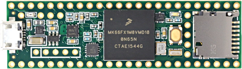
so far i stayed close to the original bluepill design (big parts on top, small parts on the bottom, 2 layer pcb)
seeing the price of the bluepill, it can’t cost that much to have something like that produced.
regarding the crystal, that’s all fine for me, i also use an smd crystal on my own boards, but stuck to the same crystals as the original bluepill for now.
regarding the usb plug, it really takes quite some extra place on the board to use a mid mounted one, unless everyone agrees that’s it’s really worth it, i’m going to stay with the top mounted one with 4 pins trough the pcb. (which happens to also be what the teensy is using according to your photo :p, probably for similar reasons)
As for the micro USB connector and crystals, these are all design choices, but if you choose to stick with original crystals, you should then keep the original connector too ![]()
Or decide to change everything at once!
If not one of these solutions, it should only be because of lack of real estate on the board.
[Squonk42 – Thu Oct 26, 2017 7:59 am] –
Yes, the Teensy is a 4-layer board with BGA components, but it is also $30…As for the micro USB connector and crystals, these are all design choices, but if you choose to stick with original crystals, you should then keep the original connector too

well no, it’s all choices XD
i chose to stick close on items that didn’t make much difference for me, and for the usb connector chose somethign more practical :p.
but i’d love to hear some other voices about this. For me it’s all the same which components we use, so far i tried to stay close to the original bluepill, but if we’d prefer a smaller smd crystal & stuff like that, why not ![]() .
.
about getting everything on 1 layer, i could give it a rough try this weekend how feasible that is (but the answer is probably not at all on 2 layers ^^’)
https://github.com/Squonk42/USBug
http://squonk42.github.io/USBug/ (please excuse the Github Pages slowliness!)
I think it is possible to achieve single-sided component load with smaller but not much more expensive parts, that will partly be gained back by a cheaper PCBA.
On the original Bluepill, the crystals, RESET button and BOOT header are HUGE and TALL: this is probably a good way to get more real-estate to move the components back on the top side.
It is also possible to switch to 0402 passives instead of 0603, except for the ones that could be removed/changed by user.
And on such a small board, having a VCC and a GND layer is not the best thing, given the few VCC required connections: it is usually better to have 2 GND planes with via stitching, and route VCC as (large) traces.
For deliverable, I think it is acceptable to provide both headers and SWD headers unsoldered, especially if we burn the bootloader into the chip, this could save some hand-soldering steps during manufacturing.
C4, C7, C8, C9, C17, C18 and C19 can be placed not far away from their respective pin. Of course, this will require some trace shuffling…
Can you also back up your ideas with some facts (that all the components on a single side is that much cheaper to produce, that the design with on both sides groundplanes that are stitched (and then just normal traces for the vcc) is better, etc…)
I’m still fairly new in this pcb designing, and this is all very interesting, but when starting out with this and wanting to read up on it, i encountered very interesting discussion on these topics, but they mostly ended in self proclaimed experts contradicting eachother, and not really helping me much in finding out which way is the way to go >_<….
So if you’ve got good sources for choosing for those design decisions, i’d love to hear them, it’s hard finding good information on this stuff, and i love all the feedback i’m getting hear as it’s a great chance to learn ![]() .
.
I design PCBs for more than 25 years professionally, using several ECAD systems. I already did simple boards like these, or much more involved boards with RF routing, matched length, antennas, high speed circuits, etc.
I posted links to an equivalent board I did with EagleCAD 6 years ago as a training while I was learning Eagle, so you can judge.
PCB design and manufacturing is not a science, it is a technology, so don’t expect clear cut answers to your questions. Most of what you will get will be based on past experience and not on rules engraved in stone.
The single-sided load for components should be obvious: when using reflow oven soldering, you will need to perform 2 operations, or to glue the components using epoxy on the bottom side, or they will just fall off… This means twice the time in the factory, this will of course cost more.
Wave soldering will have the same problem, plus the additional restrictions on the footprints that depend on the wave direction, so nobody is using it for small SMDs, it is now almost used for TH component only boards.
As for Through-Hole reflow processing (known as Paste-In-Hole), it is rather complex to set up, so Chinese PCBA factories are generally soldering them by hand after reflow soldering (cheaper), adding an extra steps and of course, costs.
As for power/ground planes, you are right, it is usually good to have the largest possible power supply plane to have an equipotential voltage that can be distributed all over the board, same for ground.
However, there is no definitive rule here: it is good to have both planes, and as large as possible, but without trace cutting these planes in half, as this almost destroys all the benefit of it. For this reason as well as for better EMC handling, it is even thus better to use 4 layer boards and have both planes in the inner layers without internal traces. For high-speed differential signals like PCI @ 2.5/5 Gbit/s, it is almost mandatory to put these signals into inner layers with stackups containing a minimum of 8 layers, or route them on the external layers and shielding everything externally.
But for small boards with only 2 layers like these, the most important is to have the largest possible ground surface as it is impossible to have a good full ground plane without trace on 2 layers, mainly for better EMC, ESD evacuation and ease of layout. A good way to do it is to use 2 under-optimal (e.g. with traces) ground planes and stitch them for the best equipotentiality. There are not many high-power components to feed on such a board, so a star or bus-like power supply distribution is OK, and the only thing to really take care of is to properly filter the analog power supply using a ferrite bead at a single point of connection with the digital supply, unless you have high-power analog needs that will dissipate too much power in it.
As for good sources, you can start by reading the IPC-7351 standard (“Generic Requirements for Surface Mount Design and Land Pattern Standard”), continue by reading all other IPC standards, as well as browsing the ARRL Handbook, among other things.
Then, with around 10 years of practice, you will start to forge your own rules ![]()
BTW, I found advises from @lkcl for handling manufacturing to a Chinese company very close to my own experience in order to avoid problems!
[Squonk42 – Sat Oct 28, 2017 1:19 pm] –
To be treated as a self-proclaimed expert is a little bit vexing, I hope it was not intentional.
i thought i worded it as well as possible not to say you are a random self proclaimed expert XD (just that it’s hard to find good info since people indicating they know it all continue to contradict eachother whenever you read discussions on how to do grounding, where to put bypass caps, … >_<).
But did want to know where you got your info from, as i’m still learning all this, and want to know where all the suggestions are coming from (and if they’ve been tried & proven, or just personal preference ![]() ).
).
And that the 2 layer components requires more work is indeed obvious, but seeing a bottom price bluepill board have it (and knowing that things that once were expensive no longer are), that’s then part of the question ![]() . is it worth it going single side components if the cost difference is maybe negligible these days? (also a problem with engineering, it’s not because it obvious that it’s the best way to go. As a programmer i know the dangers of premature optimization XD)
. is it worth it going single side components if the cost difference is maybe negligible these days? (also a problem with engineering, it’s not because it obvious that it’s the best way to go. As a programmer i know the dangers of premature optimization XD)
i’m certainly taking into account your suggestions, and indeed, it’s probably also partially an art, not an exact science (as is a lot of engineering). it’s just hard to find good references on good practices with everyone saying their solution is best for different reasons ^^’.
And thanks for the nice reply ![]() . Sorry if i vexed you, but if i don’t at least ask these questions it becomes really hard to filter all the input (since it’s usually 1 person offloading all their suggestions, and noone confirming or agreeing with anything ^^’)
. Sorry if i vexed you, but if i don’t at least ask these questions it becomes really hard to filter all the input (since it’s usually 1 person offloading all their suggestions, and noone confirming or agreeing with anything ^^’)
Concerning the SMD components, i also prefer smd crystals over the through hole ones ![]() . so i’ll have a look at updating that too (assuming noone has a good reason to stick to the bigger ones (easier to replace etc… is that required?)), it’s more compact, and if it’s another step less, the better.
. so i’ll have a look at updating that too (assuming noone has a good reason to stick to the bigger ones (easier to replace etc… is that required?)), it’s more compact, and if it’s another step less, the better.
[Squonk42 – Sat Oct 28, 2017 1:19 pm] –
I design PCBs for more than 25 years professionally, using several ECAD systems…
Hi Squonk42,
your post is really very interesting! I found some confirmations to some my “thoughts” about PCB design…
Thanks a lot for sharing! ![]()
[racemaniac – Sat Oct 28, 2017 7:48 am] –
@Squonk
Can you also back up your ideas with some facts (that all the components on a single side is that much cheaper to produce,
it’s that much cheaper to produce. think about it: the board has to go twice through a pick-and-place machine, twice with the squeegee to wipe solder paste across the stainless steel laser-cut mask… which you now have to pay for two of them not one…
but there’s quite a lot of downward-force applied: they put pins underneath along regular intervals to support the PCB to stop it bending: the 2nd time they have to b extra-careful about where to put those… because now there’s components on the board!
nut the 2nd time they can’t use the standard technique (just bake the board), they have to use something different (i forget what it is) but basically if tthey stick the board in a standard cheap oven the components on the other side will fall off! so the heating profile has to be.. different, i.e. more costly, i don’t know the precise details, but it stops the 1st set of components falling off.
all that has to have extra care *not* just “it’s twice as long therefore it’s twice the cost”, where instead for single-sided, you chuck it in the squeeger, chuck it in the pick-and-place, chuck it in the oven and it’s done.
racemaster if you want to learn more, look up “factoryforall.com”, that’s tully, he worked on the openmoko and decided to stay in shenzhen, set up his own factory and bought his own equipment, actually he would be a great person to use for manufacturing this board. his website’s extremely informative and very entertaining at the same time. say hi from me if you contact him.
[lkcl – Sat Oct 28, 2017 8:38 pm] –[racemaniac – Sat Oct 28, 2017 7:48 am] –
@Squonk
Can you also back up your ideas with some facts (that all the components on a single side is that much cheaper to produce,it’s that much cheaper to produce. think about it: the board has to go twice through a pick-and-place machine, twice with the squeegee to wipe solder paste across the stainless steel laser-cut mask… which you now have to pay for two of them not one…
but there’s quite a lot of downward-force applied: they put pins underneath along regular intervals to support the PCB to stop it bending: the 2nd time they have to b extra-careful about where to put those… because now there’s components on the board!
nut the 2nd time they can’t use the standard technique (just bake the board), they have to use something different (i forget what it is) but basically if tthey stick the board in a standard cheap oven the components on the other side will fall off! so the heating profile has to be.. different, i.e. more costly, i don’t know the precise details, but it stops the 1st set of components falling off.
all that has to have extra care *not* just “it’s twice as long therefore it’s twice the cost”, where instead for single-sided, you chuck it in the squeeger, chuck it in the pick-and-place, chuck it in the oven and it’s done.
racemaster if you want to learn more, look up “factoryforall.com”, that’s tully, he worked on the openmoko and decided to stay in shenzhen, set up his own factory and bought his own equipment, actually he would be a great person to use for manufacturing this board. his website’s extremely informative and very entertaining at the same time. say hi from me if you contact him.
i know why it *should* make a huge difference, but i’m wondering if it really *does* make such a difference if dirt cheap boards have components on both sides ![]() .
.
but i’m atm giving it a go routing it with all components on 1 side, lets see if that works out ![]()
makes me think of something i recently read on hackaday: back in the days you had to pay per via, so via optimization was important. now if they’re not too small, it doesn’t really matter anymore ![]() . it also makes sense that wearing out their drills should cost extra, but it doesn’t (anymore).
. it also makes sense that wearing out their drills should cost extra, but it doesn’t (anymore).
[lkcl – Sat Oct 28, 2017 8:38 pm] – racemaster if you want to learn more, look up “factoryforall.com”, that’s tully, he worked on the openmoko and decided to stay in shenzhen, set up his own factory and bought his own equipment, actually he would be a great person to use for manufacturing this board. his website’s extremely informative and very entertaining at the same time. say hi from me if you contact him.
Oh yes, I forgot about him!
Yes, very informative website indeed!
Here are some more resources specifically on PCBA from PCBCart:
https://www.pcbcart.com/article/content … ction.html
https://www.pcbcart.com/article/content … ocess.html
e.g. “What are Fiducials?” on this page http://www.factoryforall.com/pcba-fabrication
srp
[lkcl – Sat Oct 28, 2017 8:38 pm] – it’s that much cheaper to produce. think about it: the board has to go twice through a pick-and-place machine, twice with the squeegee to wipe solder paste across the stainless steel laser-cut mask… which you now have to pay for two of them not one…
I do not have any skills in automated PCB produvtion and it doesn’t interest me in any way, but..
Why the hell are mostly all dirt cheap Arduino/STM Pills 2component sided?
Why have the cheapest Arduino clones gigantic crystals?
Or other way round..why is my only 1sided Uno clone (Robotdyn – excellent quality) not the cheapest?
And yes, I’m wondering about the main crystal on my blue pills.. all soldered manually ![]()
Why have the cheapest Arduino clones gigantic crystals?
The 2component sided does not necessarily mean “expensive”. The top and bottom solder paste can be applied in 1 step. The bottom side parts may be glued to the pcb during pick and place. Imagine a 0.1mm drop of a glue placed by p&p machine which hardens within 1-2 secs when exposed to ultraviolet light. You place thousands parts on the bottom side and then you make a “blink” with UV light source. That is all..
Gigantic crystals are used because they are cheaper.
I guess if the size of the caps is halved etc, and more expensive small SMD crystal(s) are used it may be possible, but I wonder if the overall cost would be increased by needing to use a fab house that could build with ultra small SMD components etc.
Also the regulators need a big heat sink area of the PCB and I’m not sure thats possible on the top of the board
[racemaniac – Sat Oct 28, 2017 9:15 pm] – i know why it *should* make a huge difference, but i’m wondering if it really *does* make such a difference if dirt cheap boards have components on both sides
but i’m atm giving it a go routing it with all components on 1 side, lets see if that works out
It does take more steps, please check http://www.surfacemountprocess.com/comp … limit.html:
In the Bluepill case, bottom side is side B with only small resistors, caps and small LDO, all without epoxy glue as they are small, then the big components (MCU, 32kHz crystal, micro USB, button and fragile plastic LEDs) on top side (A).
The jumper blocks, 8 MHz crystal and SWD header are then manually soldered (you can tell because of the flux residue around the pins on the bottom side, they don’t even care to clean it).
Add 2 rows of 20-pin headers along with the board and seal it in an anti-static bag.
The original Bluepill board was designed and manufactured by VCC-GND, the price is 18.90RMB ($2.84). But you can find dirt cheap clones down to 7.35RMB ($1.11), when the cheapest STM32F103C8T6 chip you can find is at 7.00RMB… As you can see, the price is very subjective! It depends if you get new or used (possibly defective or untested) parts, non-RoHS process, (non-)testing, grey shift assembly and/or bad working conditions, etc.
If you want to stay with decent assembly conditions, RoHS (you have to!) and (mostly) controlled part origin, then you will find that everything has a price. The manufacturer may not say so, but in the end, they will charge you more ![]()
[racemaniac – Sat Oct 28, 2017 9:15 pm] – makes me think of something i recently read on hackaday: back in the days you had to pay per via, so via optimization was important. now if they’re not too small, it doesn’t really matter anymore
Chinese PCB manufacturers no longer charge for more vias, as they found that it is almost proportional to the board area. You can play with online PCB quoting forms like SeeedStudio Fusion to see what really matters today.
As for the 32 kHz crystal, we can either leave the bulky SMD MC-306 one, or replace it by a smaller FC-135 package with known CL (12.5pF)
The BOOT header will have to be replaced by a tactile button, like in the Mapple Mini. The smallest and cheapest I know is the ALPS SKSGACE010, also used in the NodeMCU board. Like the Mapple Mini, you can also connect it to a GPIO (PB8) through a 0R to get a free USER button…
The DMP2160UW PMOS is a good idea to get a low-drop diode.
The SY6280 is good and very cheap. A TPD3S0x4 combined USB Current Limit Switch and D+/D– ESD Protection like in the Teensy 3.6 would be nice to have, but too expensive. For a dev board where you can touch all chips with your fingers, ESD is not really a concern (you do wear a wrist ESD strap, don’t you? ![]() ).
).
Please don’t use a precious PC9 pin for the USB switch enable pin: it is part of the few pins that can provide SDIO interface functionality, so we would better use a dumb pin like PC0 or PC1 for this purpose. My idea would be to add an optional MicroSD socket on the (now flat) bottom side routed like the MicroPython board. Refer to my previous post you may have missed. Now, you know why I insist on having all components on top ![]() .
.
I think that both SDIO and I2S could be very interesting additions to the standard STM32F103C8T6 Bluepill, meaning that PD2 and PC8-12 should be used for the optional onboard SDIO connector, and PC6-7 for the only available I2S MCK pins as TH pads…
Don’t forget that STM32F103RBT6 are almost pin-to-pin compatible with STM32F405RGT6 64LQFP package and cost the same price as the STM32F103C8T6… Provided we take care of the VCAP pins (replace 2u2 caps by 0R for F103) and add an optional USB pull-up on PA12. We may then have 2 versions of the board sharing the same PCB, one with F103, one with F405.
Optionally run the SPI to the SDIO socket? Maybe too many troubles, but would be nice to have for F103.
BTW, pin 1 of bottom edge header should be VBAT (i.e., on the SWD header side, not near the micro USB connector).
i’m going to give it a try, but not sure if it’ll be possible with 8/8mil routing & 0603 smd parts.
for crystals i was thinking of going for a 5032 8Mhz crystal, and for the 32k i even found some good 2012 crystals (they’re really small, love it
btw, before i take a “wrong” micro sd slot, which one would you guys recommend? ![]()
You prove that it is possible to keep the same form factor with only minimal changes. Now with more involved component selection and single-side PCB routing, we could keep the price reasonable and pack as much feature as possible.
We can use 6 mils/6 mils/0.3mm PCB manufacturing at no additional cost, this is considered in China as the “PCB prototype quality”, like you can find at most online PCB vendors (see SeedStudio above), so it is reasonable to go down to these specs.
We should seriously consider if we keep the original PCB dimensions of 2.1″ x 0.9″ (53.24mm x 22.86 mm), or if we reduce it a tad to match the recommended 50 mm used by most of the cheap PCB houses… This may perhaps help reduce the cost, or at least it will reduce it for those willing to DIY, because we could panelize 2 of them in a 50 mm x 50 mm square.
Keeping 0603 parts for small resistors and caps <= 100nF is a choice: do we go for 0402 or do we keep the ability to perform DIY soldering with minimum soldering skills? This won’t save a lot of real estate, but this may help greatly to place parts in a more optimal way.
For the crystals, the most difficult is to find parts with a specified CL, which is seldom the case on TaoBao or Aliexpress.
Regarding the microSD socket, look at 104031-0811 from Molex. Only 11.95 mm wide, meaning that it fits between the BP rows of pins… And you can find it cheap on TaoBao from many vendors.
with its 20 pins length, it’s just a bit too big to get down to 50mm….
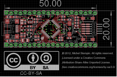
- USBugSmall.png (126.82 KiB) Viewed 186 times
I think it works because it looks like the limits set from copper to board edge is not so strict (some manufacturers do not specify it) and depends on the PCB feed direction: the PCB are moved between 2 parallel rails that are either ~6 cm (5 + 2 * 0.5 mm) or ~11 cm (10 + 2 * 0.5 mm) apart:
This is why prototypes services are so strict on dimensions (5 cm or 10 cm), they don’t want to set up the rails for each new board! Then the other dimension is set to 5 cm or 10 cm too, probably for convenience during storage.
Our edge connectors are 20 x 0.1″ = 2″ =5.08 cm long, so when you round them to 5 cm, you cut their last copper pads at the extremities by only 0.04 mm (1.6 mil) each, and as we are cutting perpendicular to the rails above, it should be OK.
BTW, should we keep the PCB area outside the 2 rows of header with silkscreen pin legend or not? They end up wasting 1 breadboard hole on each side of the PCB…
I had the opposite idea about the length…
If there is not enough space on the top of the PCB it could probably be increased by 2 or perhas 3mm at each end, as its unlikely that anyone who has built a board that houses the Blue Pill would have squeezed it in that tightly.
I dont think placement of the SWD connector is critical, and you could drop the Vcc and Gnd pins on that header, as both those connections are available elsewhere.
@squonk42
Thanks for the heads up about the SDIO pins etc.
SDIO and I2S are important as they are not available on the F103C8
Re:resistor size that allows hand soldering.
I don’t think this is necessary
Removing even the smallest SMD resistirs isnt that hard using a soldering iron, as in my experience they seem to stick to the solder and flux and just come away from the board when you remove the iron.
I cant think of any circumstances when people would want to replace resistors
Re:Pads for unised MCU GPIO pins on the bottom of the board.
Hakimg back to the Teensy… We could do this if no components were on the bottom of the board
Re:regulator
I thought there were heat dissipation issues unless the regulator was on the back of the board where there was a lot of copper to dissipate the heat ??
[RogerClark – Sun Oct 29, 2017 9:21 am] –
Looking at the last design posted by @racemaniac in the PCB 3D viewer, I think its going to be a tough job to get all the components onto the top of the PCB.I guess if the size of the caps is halved etc, and more expensive small SMD crystal(s) are used it may be possible, but I wonder if the overall cost would be increased by needing to use a fab house that could build with ultra small SMD components etc.
Also the regulators need a big heat sink area of the PCB and I’m not sure thats possible on the top of the board
It is possible using small crystals and buttons, still using huge 0603 passives (sorry, still using EagleCAD):
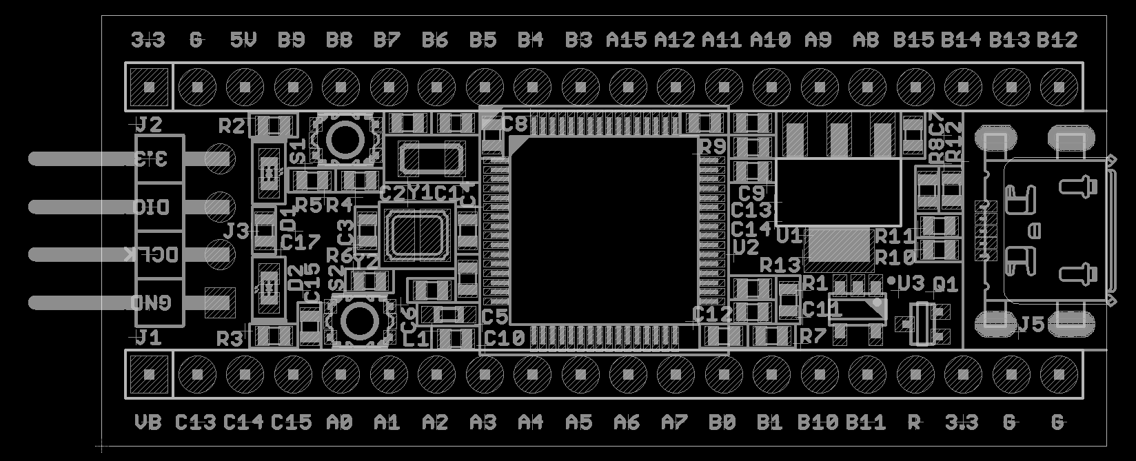
- BluePillF4.png (55.59 KiB) Viewed 168 times
[RogerClark – Sun Oct 29, 2017 9:32 pm] – Re: PCB lengthI had the opposite idea about the length…
If there is not enough space on the top of the PCB it could probably be increased by 2 or perhas 3mm at each end, as its unlikely that anyone who has built a board that houses the Blue Pill would have squeezed it in that tightly.
Well, I agree we could extend the board in length, the 5 cm limit comes from the cheap prototype PCB houses that use this as a billing threshold.
[RogerClark – Sun Oct 29, 2017 9:32 pm] –
I dont think placement of the SWD connector is critical, and you could drop the Vcc and Gnd pins on that header, as both those connections are available elsewhere.
Yes, good idea, just right next to the SWD connector!
[RogerClark – Sun Oct 29, 2017 9:32 pm] – @squonk42Thanks for the heads up about the SDIO pins etc.
SDIO and I2S are important as they are not available on the F103C8
Yes, and even better: if we use PC10 for SDIO_D2, PC11 for SDIO_D3/CD and PC12 for SDIO_CK, they just happen to match USART3_TX, USART3_RX and USART3_CK, respectively on the STM32F103Rx, this means that we could possibly drive the SD Card in SPI for the 103! ![]()
[RogerClark – Sun Oct 29, 2017 9:32 pm] – @squonk42
Re:resistor size that allows hand soldering.I don’t think this is necessary
Removing even the smallest SMD resistirs isnt that hard using a soldering iron, as in my experience they seem to stick to the solder and flux and just come away from the board when you remove the iron.
I cant think of any circumstances when people would want to replace resistors
OK, then we will move down to 0402 for all passives except caps > 100n.
[RogerClark – Sun Oct 29, 2017 9:32 pm] – Re:Pads for unised MCU GPIO pins on the bottom of the board.Hakimg back to the Teensy… We could do this if no components were on the bottom of the board
Yes
[RogerClark – Sun Oct 29, 2017 9:32 pm] –
Re:regulatorI thought there were heat dissipation issues unless the regulator was on the back of the board where there was a lot of copper to dissipate the heat ??
The AP2114AH in SOT223 package has a Tja of 128°C/W without heatsink, and the STM32F405 has a max current draw of 450mA. When powered from 5V, the heat dissipated will be (5V – 3.3V) * 0.45A = 0.4W, or a 52°C rise in temperature above ambient, all with a drop-out voltage that will allow for powering from a LiPo battery (450mV DO @ 1A), even less dissipated heat when powered from battery. We cannot feed a nuclear power plant, but we have some room for powering external stuff before frying the LDO.
OTOH, I benefit from my existing part library!
Here is my current schematic for open discussion.
- BluePill F4 Schematics.pdf
- (58.07 KiB) Downloaded 30 times
thez programming header/crystals/analog rail side was ok to do (btw, that’s one difference between your schematic and mine: on one of the 3v3/gnd parts on the pins, i break out the analog 3v3/gnd instead of the regular one, so they are also available on the headers.)
although i have some parts there i still really need to improve.
the other side with boot selection/button/big voltage regulator/… isn’t working out for me so far ^^’
Plus, you don’t have to put the buttons on the USB side like the original, you can move them on the SWD side if necessary (see my part placement above).
Breaking out the analog VCC/GND on header is a good thing, but it breaks the compatibility with existing Bluepill boards, @RogerClark: what do you think?
In my schematics, I just dropped the LDO providing the analog power supply: this is a luxury IMHO. Better have a good ferrite bead between +3V3 and +3V3A only to filter high-frequency noise, and have (as much as possible on such a small board) separate GND and GNDA only connected at a single point, which is the normal way to handle analog/digital coexistence. Adding a ferrite bead between GNDs is not necessarily a good thing for small signals, as it will create a voltage offset between GNDs that depend on ground currents, better put a trace only.
But you could add another pin (through hole) somewhere else, or just a pad on the underside etc
*edit*
after thinking about it a bit more, aren’t both options incompatible?
If i don’t put the analog 3v3 on the standard header, anyone feeding their bluepill via the standard header and doing something analog is out of luck, since the analog part won’t be powered at all.
at least for my solution, if you provide power via both 3v3 pins, the entire board is powered. now i don’t have any bluepill shields/projects that rely on this, so not sure what people who expect pin compatibility are expecting, but i think my solution also has some merits.
the only other option would be a jumper to connect 3v3a with 3v3 (or a small solder bridge you can make, a jumper would be a bit big), and then just keep the regular 3v3 on both pins.
Yes. I guess it would be possible to use one of the Vcc’s as analog Vcc.
Are you using a really small regulator for analog Vcc, or is it roughly equivalent to the cheap regulator on the Blue Pill ?
What advantage is there to having the analog vcc available for external circuits?
Lower noise than the main regulated output ?
I suspect people may use the Vcc pins to power a lot of things and existing designs may link them in their PCB, or assume they are connected together internally.
[RogerClark – Mon Oct 30, 2017 9:59 am] –
@racemaniacYes. I guess it would be possible to use one of the Vcc’s as analog Vcc.
Are you using a really small regulator for analog Vcc, or is it roughly equivalent to the cheap regulator on the Blue Pill ?
What advantage is there to having the analog vcc available for external circuits?
Lower noise than the main regulated output ?I suspect people may use the Vcc pins to power a lot of things and existing designs may link them in their PCB, or assume they are connected together internally.
for analog i’m using the small ap2112 (the one i originally used for the non analog part too, but that was found to be too light).
and there is no very specific reason to have the analog 3v3 also available on the pin headers (other than it at least being reachable/connectable if you’re not using a 5v supply).
it seems we’ve found another design decision to make:
– keep the original pins (both just 3v3, the analog supply then maybe on other pins) -> not quite a fan of this honestly. taking up quite some extra space for this…
– my solution of having the 3v3a & gnda on the pins next to the programming header -> probably also not ideal, depends on how the original bluepills are used (if they power via both 3v3 pins, it’s compatible (as both grounds are tied together via a ferrite bead), otherwise they’d have to make sure to power the other 3v3 pin too)
– keeping the original pins, but offering a jumper/solder bridge that can be made to tie the 3v3 to 3v3a -> very compatible, but it’s less elegant if you want to provide your own analog 3v3 rail (you can connect your 3v3a to the appropriate pin of the jumper/solder bridge, but the analog ground isn’t really broken out in this case…)
– probably some other options i’m not seeing yet ^^’
each choice has its advantages & disadvantages, kepping 100% compatibility is impossible if we now have a separate analog 3v3, so we’ll have to pick our compromise ![]() .
.
From AN2586 “Getting started with STM32F10xxx hardware development”:
Power supply schemes

The circuit is powered by a stabilized power supply, VDD.

● Caution:

– If the ADC is used, the VDD range is limited to 2.4 V to 3.6 V

– If the ADC is not used, the VDD range is 2.0 V to 3.6 V

● The VDD pins must be connected to VDD with external decoupling capacitors (one

100 nF Ceramic capacitor for each VDD pin + one Tantalum or Ceramic capacitor (min.

4.7 µF typ.10 µF).

● The VBAT pin can be connected to the external battery (1.8 V < VBAT < 3.6 V). If no

external battery is used, it is recommended to connect this pin to VDD with a 100 nF

external ceramic decoupling capacitor.

● The VDDA pin must be connected to two external decoupling capacitors (100 nF

Ceramic + 1 µF Tantalum or Ceramic).

● The VREF+ pin can be connected to the VDDA external power supply. If a separate,

external reference voltage is applied on VREF+, a 100 nF and a 1 µF capacitors must be

connected on this pin. In all cases, VREF+ must be kept between 2.4 V and VDDA.

● Additional precautions can be taken to filter analog noise:

– VDDA can be connected to VDD through a ferrite bead.

– The VREF+ pin can be connected to VDDA through a resistor (typ. 47 Ω).
Well beyond what a small ferrite choke could clean up.
The amplifier was for a HB100 doppler radar module, and I have since found a better design for the amplifier which uses its own regulator to minimise the noise.
IMHO, I think before the analog Vcc regulator was removed, we would need to make sure its definitely not needed, by doing some practical validation on real hardware.
- Decoupling Insertion Loss.png (36.85 KiB) Viewed 354 times
[Squonk42 – Sun Oct 29, 2017 12:47 pm] –
Regarding the microSD socket, look at 104031-0811 from Molex. Only 11.95 mm wide, meaning that it fits between the BP rows of pins… And you can find it cheap on TaoBao from many vendors.
no. not that one. it’s more expensive and not as ubiquitous in the futian district. molex is also known for being way overpriced.
use the one known as “TF Card”, push-push, with the footprint below:
- Untitled.jpg (17.41 KiB) Viewed 350 times
I also consider it as a not mounted option with only a provision for the footprint by default.
Now if you can find a cheaper one having width < 500 mils (12.7 mm), I take it ![]()
EDIT: maybe this one or these simpler no push-push ones will do, difficult to tell, there are no dimensions. If someone can ask the vendors for a 2D drawing…
- 104031-0811.png (20.19 KiB) Viewed 336 times
i have most types of micro sd slots in my collection (it’s cheap, and the best reference if you want to use them is actually having one to measure XD).
A 600ohm Ferrite Bead does not have 600ohm “resistance”. That “600ohm” is “impedance – mostly an inductive reactance” at some frequency (ie 100MHz). Ferrite beads have got 0.0xx ohm DC resistance typically..
Even with 600ohm/100MHz impedance and the ADC’s bandwidth (could be ~1MHz) the FB will not have any significant impact on the 1LSB variation (as the FB’s impedance at 1MHz would be maybe 2-5ohm)..
PS: there are smd “inductors” and smd “feritte beads” available.
The inductors are rated in uH or nH, while FBs in “ohms” (an impedance at 100MHz).
Use FBs only, as the “inductors” have got large DC resistance (0.x to ~ohms) and low self-resonance (~1-100MHz) such they will ring…
Also you want to use an FB with rather lower impedance (ie 30-100ohm) as the larger values will peak as well (they do self-resonate at >=200MHz)..
– try to make the pcb with all components on 1 side (even though i haven’t got confirmation yet that it will make a worthwhile price difference. Since there are many cheap boards with caps & small components on the bottom) -> anyone got some hard facts about the price difference (not just reasons why it *should* be more expensive, but an example of actual quotes that show this?).
– if possible, make room for an sd slot (need to find one that is small enough). is going to be hard though (the routing of this & the above will be very complex)
– 2 voltage regulators, or just 1 with ferrite beads & caps connecting digital & analog lines? -> i assume the original maple mini did the effort of 2 voltage regulators for a reason?
– trying to break out as many pins as possible (probably as SMD pads then, even if that is less sturdy. 2mm/1.27mm spaced trough hole pads is also an option to save some space)
– trying to make the board 5cm long (even though the pads on the end are then too close to the edge. the manufacturer will have to ignore that)
– which resistors to include on the usb port? (make room for 1k5 pullup in case of an 103 chip? is it worth putting the 22R resistors on the dp & dm lines?
– go with a midmount usb connector? (-> would be more robust, but means we have less space for routing the usb lines…)
The consensus, was this is not needed on the F4
Re: USB 22ohm resistors.
i think this is best practice, but optional, depending on space on the PCB
Re: Regulator for analog Vcc
I presume that Leaflabs had a good reason for using the second regulator. I suspect, its potentially cheaper and takes less space on the PCB than the passive components you would need instead
Re: 50 mm long board and components in bottom of board
I think with too many constraints, the board is going to take months to design and may never get produced.
Perhaps move as many as possible to the top without wasting hours of time and potentially adding conflicts to the PCB
[RogerClark – Tue Oct 31, 2017 8:17 pm] –
Re: USB pullupThe consensus, was this is not needed on the F4
Yes, but if you make a provision for it, along with replacing the 2x VCAP capacitors by 0R shunts, the board is then compatible with all LQFP64 STM32s, including L4s, and including the SD Card connector through SPI… I think it is really worth the pain!
[RogerClark – Tue Oct 31, 2017 8:17 pm] –
Re: USB 22ohm resistors.i think this is best practice, but optional, depending on space on the PCB
Agreed, this is usually a provision for CEM certification by replacing with a CMC or adapting the values to get a better eye-diagram for USB certification. Not needed, but we may keep it if we have enough real estate on the board.
[RogerClark – Tue Oct 31, 2017 8:17 pm] –
Re: Regulator for analog VccI presume that Leaflabs had a good reason for using the second regulator. I suspect, its potentially cheaper and takes less space on the PCB than the passive components you would need instead
Not sure, as the regulator will need at least 2x caps anyway (1x at the input, 1x at the output), and you still need at least a decoupling cap near STM32’s AVDD pin, so it is necessarily more expensive, takes more space, and dissipates more power than a passive solution. Probably Leaflabs did not think much when doing this, and just used a bazooka to kill a fly. BTW, the Mapple is the only small dev board I have seen that used a second LDO for analog supply ![]()
[RogerClark – Tue Oct 31, 2017 8:17 pm] –
Re: 50 mm long board and components in bottom of boardI think with too many constraints, the board is going to take months to design and may never get produced.
Perhaps move as many as possible to the top without wasting hours of time and potentially adding conflicts to the PCB
If the 50 mm constraint only applies to small PCB prototypes and not to the intended manufacturer, then we should get rid of it, as well as using only 0603 passive components and move down to 0402 alltogether, as this won’t be more expensive and save us some space on the board.
As for double-sided component load, it will be more expensive than single-sided, but the question is how much for the intended manufacturer again. If not too much, then we should only try to make room on the bottom side for the optional SD Card connector. This connector may be too big to be soldered economically on the bottom side, though…
Maybe we should ask the manufacturer for the price difference? If honest, they will tell us, otherwise, they will just take the max price and tell us it is the same price ![]()
As for additional pins to break out, a clever solution is to use a second row of 2.54mm holes offset by 1.27mm, like the LicheePi Zero (btw, look at their TF Card connector! It is a Molex 47309-2851, it fits between the 2 header rows):
[RogerClark – Tue Oct 31, 2017 8:17 pm] – ] Re: Regulator for analog VccI presume that Leaflabs had a good reason for using the second regulator. I suspect, its potentially cheaper and takes less space on the PCB than the passive components you would need instead
Not sure, as the regulator will need at least 2x caps anyway (1x at the input, 1x at the output), and you still need at least a decoupling cap near STM32’s AVDD pin, so it is necessarily more expensive, takes more space, and dissipates more power than a passive solution. Probably Leaflabs did not think much when doing this, and just used a bazooka to kill a fly. BTW, the Mapple is the only small dev board I have seen that used a second LDO for analog supply ![]()
The LeafLab Maple Mini was a 4 layer PCB with an analog ground plane and a separate digital ground plane. The separate voltage regulator for the analog likely was a decision made to enhance the overall low-noise floor. Most of us have come to think of the Maple Mini being the 2-layer knockoff from China.
Ray
@squonk42
I forgot about F103R compatibility.
I think this needs to be a secondary consideration, as the primary focus as F4
The MCU is on the underside of the board, along with 8Mhz crystal (in a SMD package) and the regulator and the USB reset transistors
The top has the buttons, LEDS, USB socket and other passive components.
So…
My guess is that the cost of putting components on both sides of the boards can’t be a big factor to these companies, otherwise they’d have spent a bit more time on the design and put all the components on one side.
BTW. The original LeafLabs Maple mini has components on both sides of the board as well
(there is photo of the bottom of the Maple mini on Leaflabs site)
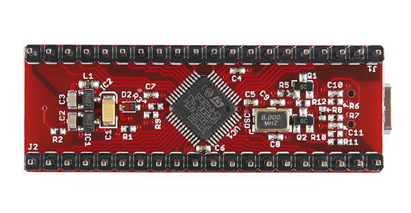
[RogerClark – Tue Oct 31, 2017 8:17 pm] – Re: 50 mm long board and components in bottom of boardI think with too many constraints, the board is going to take months to design and may never get produced.
Perhaps move as many as possible to the top without wasting hours of time and potentially adding conflicts to the PCB
tbh, personally i still prefer the bluepill solution: big things on 1 side, small things on the other.
It’s the reason why the bluepill has been the board i’ve been putting other mcu’s on. the maple mini’s pads don’t allow a qfn to fit, and the blackpill has small caps right next to the mcu, so changing the mcu means you’ll also be removing the caps, and is just annoying extra work ![]() .
.
if we want to allow for people to change crystals/mcu/… easily, making sure there are no tiny caps/resistors right next to them makes a lot of sense ![]() .
.
OK, then it is a completely different story and much more understandable, thank you Ray! Low-cost was then not the primary concern like for us here. 4-layer is more expensive.
Re: Components on both sides of the PCB
It looks like it is a cheap option, so let’s go for it!
However, I agree with @racemaniac to put all large components (what about the SD Card connector?) on top and small ones on the bottom. Plus, because of the package size, we don’t have much space to sprinkle the decoupling caps around it, putting them below the chip would be much better and also easier for replacing the chip. For crystals, this is may be different, as vias should be avoided if possible on the clock traces.
Re: F103R compatibility
Not only F103R, but all STM32 MCUs featuring the simple USB Device peripheral in LQFP64 package:
STM32L052R6 STM32L052R8 STM32L053R6 STM32L053R8 STM32L063R8 STM32L072RB STM32L072RZ STM32L073RB STM32L073RZ STM32L083RZ STM32L100R8 STM32L100R8-A STM32L100RB STM32L100RB-A STM32L100RC STM32L151R6 STM32L151R6-A STM32L151R8 STM32L151R8-A STM32L151RB STM32L151RB-A STM32L151RC STM32L151RC-A STM32L151RD STM32L151RE STM32L152R6 STM32L152R6-A STM32L152R8 STM32L152R8-A STM32L152RB STM32L152RB-A STM32L152RC STM32L152RC-A STM32L152RD STM32L152RE STM32L162RC STM32L162RC-A STM32L162RD STM32L162RE STM32L433RB STM32L433RC STM32L443RC STM32L452RC STM32L452RE STM32L462RE STM32F070RB STM32F072R8 STM32F072RB STM32F078RB STM32F102R4 STM32F102R6 STM32F102R8 STM32F102RB STM32F103R4 STM32F103R6 STM32F103R8 STM32F103RB STM32F103RC STM32F103RD STM32F103RE STM32F103RF STM32F103RG STM32F302R6 STM32F302R8 STM32F302RB STM32F302RC STM32F302RD STM32F302RE STM32F303R6 STM32F303R8 STM32F303RB STM32F303RC STM32F303RD STM32F303RE STM32F373R8 STM32F373RB STM32F373RC
This is a long dropped-compatibility list for just a small 0402 pull-up resistor, don’t you think?
Now, I agree that the Maple Mini dual transistor disconnect feature is probably a bit of overkill.
[racemaniac – Wed Nov 01, 2017 10:30 am] –
Concerning the dual supply: if we don’t go for a dual supply, can someone draw me a schematic of what we would replace it by?
See my post above: a simple PI filter with 1µF cap, 470R ferrite bead and 100nF close to the AVDD pin:

I will try to experiment this filter on a real BluePill 3.3 pin tomorrow
Other subject, I found this simple (no push-push) narrow (12.2 mm) and cheap (0.17RMB = $0.03) SD Card connector on Taobao:
https://item.taobao.com/item.htm?spm=a2 … t=4#detail
Do we need to keep the PCB overhang on the outside of the header rows? On one hand, it is convenient to silkscreen to pin name, but OTOH, it makes the board wider by 2 pins on a breadboard…
Re: VBUS valid sensing for HNP SRP
In the STM32F4 Reference Manual RM0090, page 1254, section 34.6.2, there is a mention about connecting PA9 as a VBUS sensing for HNP/SRP: googling around, I found that both SRP (Session Request Protocol) and HNP (Host Negotiation Protocol) are 2 USB OTG protocols, but does anybody knows if these are required for proper USB operation or not?
Having to connect PA9 to VBUS would be rather inconvenient, as it also has the USART1_TX function used by the ROM bootloader…
i was also doubting keeping them, but both for the labels and ease of routing, they do have their advantages.
[racemaniac – Fri Oct 20, 2017 11:28 am] – ..but i do understand that as it currently is, it’ll be easier to have actually produced by someone.
Ok, seems to be my fault, I just read the first post carefully again… now I understand all those fuckin’ Taobao links better ![]()
Nevertheless, i found some KiCad projects in here, so why not combine both, elec freak who like to solder and designs ready for production?
Resourcing for the needed component should be the problem of the producing factory(ies), normally they should know where to buy ![]()
When I must read all that stuff regarding two or multilayer, SDcard and so on..plz keep in mind the header: f4 versions of “the BluePill”!
The “BluePill” has no SD card, has two layers, 2-sided components, not the smallest.. in short: its cheap, its cheaper, its cheapest – that’s all!
[ChrisMicro – Sun Oct 29, 2017 9:01 am] –
This one ? RobotDyn?
No, as I wrote UNO
the predecessor of this one
from times when they started selling on ALI – with free shippin’ that time;)
[bianchifan – Fri Nov 03, 2017 10:20 am] – Resourcing for the needed component should be the problem of the producing factory(ies), normally they should know where to buy
Yes, but defining exactly what to buy is the designer’s problem ![]()
And to get the cheapest solution, you need to compare different sources!
[bianchifan – Fri Nov 03, 2017 10:20 am] – When I must read all that stuff regarding two or multilayer, SDcard and so on..plz keep in mind the header: f4 versions of “the BluePill”!
The “BluePill” has no SD card, has two layers, 2-sided components, not the smallest.. in short: its cheap, its cheaper, its cheapest – that’s all!
Yes, but the BluePill has some well known flaws:
- wrong USB pull-up resistor
- Bad analog power supply / ground, resulting in poor ADC performance
- Useless BOOT1 header & jumper
- BOOT0 header & jumper are huge, could be more practical to have a second button instead
Now if you go from STM32F103 to STM32F405, you got more problems:
- larger package: 10×10 LQFP64 vs. 7×7 LQFP48, doesn’t fit so easily!
- Power consumption: 240 mA vs. 50 mA max, so you need a beefier voltage regulator (at least 600 mA) to be useful, with low drop-out voltage (< 250 mV) for the board to allow powering from a 3.7V LiPo battery
Now, besides more processing power, single-precision FPU, more Flash and RAM memory, the STM32F405 also brings in some nice features:
- USB OTG: but if you want to implement Host mode, you need to provide an USB load switch
- SDIO: you need at least to break out these pins, or provide an optional SDIO socket
- I2S: here, too, you need at least to break out the additional pins
- More GPIOs: break out if possible
… All this on a 2-layer, 2-sided components, same form-factor board at the cheapest possible price: this is exactly where we are at, by weighting carefully each component and each decision together ![]()
Squonk, i like the small buttons you linked… but can’t find them anywhere on aliexpress or ebay (okay, i could find them from 1 seller at a ridiculously high price more than 1€ a piece)
Can we maybe find some buttons that are small enough and that can easily be sourced by those wanting to make their own boards?
Usually they [pcb manufacturers who offer assembly] request you to provide them with the vendor’s IDs for all the BOM parts, they source from standard sources like digikey, mouser, etc. I doubt, however, the $2 BluePill-like boards manufacturers source from those large distributors [they are expensive]. Most probably they collect the cheap surplus parts from local companies [large market with spare/surplus parts]..
However I am not sure on the setup for the pick and place machines.
Probably best to speak to a company who already manufactures a similar board.
Robot Dyn have replied to 2 of my emails about their Black Pill board, so perhaps if we placed a large enough order they may be interested.
Basically its all about the money. I can get boards hand soldered in China, but they charged around $10 each , and that was for a less complex board
[racemaniac – Fri Nov 03, 2017 4:03 pm] –
btw, concerning the buttons
Squonk, i like the small buttons you linked… but can’t find them anywhere on aliexpress or ebay (okay, i could find them from 1 seller at a ridiculously high price more than 1€ a piece)
Can we maybe find some buttons that are small enough and that can easily be sourced by those wanting to make their own boards?
I usually buy them from Mouser, but they are also available at other online distributors.
[RogerClark – Fri Nov 03, 2017 7:34 pm] –
Perhaps the best solution with the components is to initially supply them to the manufacturerHowever I am not sure on the setup for the pick and place machines.
Probably best to speak to a company who already manufactures a similar board.
Robot Dyn have replied to 2 of my emails about their Black Pill board, so perhaps if we placed a large enough order they may be interested.
Basically its all about the money. I can get boards hand soldered in China, but they charged around $10 each , and that was for a less complex board
IMHO, the best approach is to first design a board with a careful part selection, so they can be sourced cheap both from China (TaoBao is a good way to check for the best deals) and from either global online distributors or AliExpress/eBay.
The idea is to correct the BluePill flaws, take into account interesting features in more powerful chips like the F405, but without adding to the bill or over-engineering.
Then get the PCB done and assemble some prototypes by hand by as many volunteers in this forum as possible to debug the design and correct hardware bugs.
And eventually, we could approach some manufacturers with gerber and BOM files, and ask them for the cost of sourcing, PCBA, bootloader flashing, storage and shipment from AliExpress/eBay/Amazon direct from China. Maybe charge a small extra fee to pay your server and electricity bill, Roger ![]()
[Squonk42 – Fri Nov 03, 2017 9:26 pm] –[racemaniac – Fri Nov 03, 2017 4:03 pm] –
btw, concerning the buttons
Squonk, i like the small buttons you linked… but can’t find them anywhere on aliexpress or ebay (okay, i could find them from 1 seller at a ridiculously high price more than 1€ a piece)
Can we maybe find some buttons that are small enough and that can easily be sourced by those wanting to make their own boards?I usually buy them from Mouser, but they are also available at other online distributors.
that’s great, but i’m from europe ^^’
buying from the likes of mouser/digikey/… is pretty expensive in shipping fees for me ^^’
but after looking i actually found 1 aliexpress seller selling it at a good price: aliexpress link
Besides the measurements, isntead of giving the part number in the description, it’s the name of the photo -_- (thanks google for finding that)
[racemaniac – Sat Nov 04, 2017 6:47 am] –[Squonk42 – Fri Nov 03, 2017 9:26 pm] –
I usually buy them from Mouser, but they are also available at other online distributors.that’s great, but i’m from europe ^^’
buying from the likes of mouser/digikey/… is pretty expensive in shipping fees for me ^^’
Me too ![]()
[racemaniac – Sat Nov 04, 2017 6:47 am] – but after looking i actually found 1 aliexpress seller selling it at a good price: aliexpress link
Besides the measurements, isntead of giving the part number in the description, it’s the name of the photo -_- (thanks google for finding that)
Thank you for sharing the link. We are lucky, this button is used in BMW/Mercedes car keyfobs!
so.
that’s one possible outlet and he has several westerners visiting him because he’s known to either have stuff in stock, or he and his brother can order it for you. i think he’s a really good person to know. so! once this board is up and running i’ll make sure he gets some to sell.
i hope to soon resume work on this
bit of a break now (had some holidays, lots of social events atm ^^’)
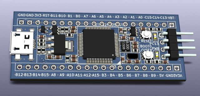
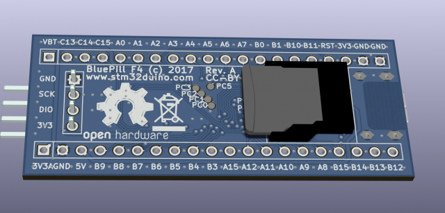
you’re routing that in 2 layers? XD
[racemaniac – Tue Nov 28, 2017 7:04 am] –
woow, nice!
you’re routing that in 2 layers? XD
Thanks!
Yes, 2 layers, 6 mils trace width / 6 mils spacing, 6 mils annular ring and 12 mils (~0.3 mm) min holes, passed DRC/ERC!
[Pito – Tue Nov 28, 2017 8:12 am] –
How many free holes along the edges you get when you insert it into a solderless breadboard?
It is the same form factor and pinout as the “original” BluePill, i.e. 2.1″ x 0.9″.
[Squonk42 – Tue Nov 28, 2017 8:17 am] –[racemaniac – Tue Nov 28, 2017 7:04 am] –
woow, nice!
you’re routing that in 2 layers? XDThanks!
Yes, 2 layers, 6 mils trace width / 6 mils spacing, 6 mils annular ring and 12 mils (~0.3 mm) min holes, passed DRC/ERC!
that’s then 24mil vias?
i think most cheap services specify 25/27 mil vias with 12 mil drill (although, a service like dirtypcb probably will just build it like that, some others may actually refuse it from what i heard)
i’m very curious to see how you routed all that XD. (and glad someone else is helping out, i’ve got too many electronics projects happening ^^’. it’s becoming a fulltime job)
[racemaniac – Tue Nov 28, 2017 9:12 am] –
that’s then 24mil vias?
i think most cheap services specify 25/27 mil vias with 12 mil drill (although, a service like dirtypcb probably will just build it like that, some others may actually refuse it from what i heard)
i’m very curious to see how you routed all that XD. (and glad someone else is helping out, i’ve got too many electronics projects happening ^^’. it’s becoming a fulltime job)
I used SeeedStudio Fusion PCB Service with these specs, 0.3 mm min hole + 6 mils OAR, $15.05 for 10 panels of 5 PCBs (fitted on 10 cm x 10 cm):
http://support.seeedstudio.com/knowledg … cification
something to look forward to XD
[Squonk42 – Tue Nov 28, 2017 12:41 pm] –
@RogerClark: I cannot attach the 877 KB ZIP file to a post, how may I proceed?
weren’t the files already being committed to the github repo? maybe create a pull request to the stm32duino github
[Squonk42 – Tue Nov 28, 2017 12:41 pm] –
@RogerClark: I cannot attach the 877 KB ZIP file to a post, how may I proceed?
Share over google drive?
The hosting has space limits which I am already pushing up against and I do not want to have to spend more on hosting this site.
(I know I could move hosts etc, but this is not the only site i run in this hosting plan and it would take days to move it all and reconfigure )
https://drive.google.com/open?id=15XfdO … 3djr8sFks6
As this is my first design using KiCAD, please accept my mistakes!
The design uses only 0603 passive SMT components, and I routed the board on 2 layers using 6 mils trace width / 6 mils spacing, 6 mils annular ring and 12 mils (~0.3 mm) min holes constraints and passed DRC/ERC.
It should have most of the features discussed previously in this thread, plus some more:
Form factor:
- same form factor as “original” BluePill: 2.1″ x 0.9″ (53.34 mm x 22.86 mm)
- same pinout, except for corner +3.3V, replaced by backward-compatible +3.3VA (Analog power supply)
Power supply:
- ultra low-drop, high current (1A) AP2115HA-3.3TRG1 LDO, compatible with standard 1117 LDO pinout, but should work with +3.7V LiPo batteries
- optional AP2112K3.3-TRG1 LDO for Analog power supply or cheaper CLC filter with ferrite bead
LEDs:
- 1 green LED for POWER
- 1 red LED connected to PC13
Buttons:
- 1 miniature RESET switch button
- 1 miniature BOOT0 switch button, can be tied to PB8 using a shunt resistor (default, like Maple Mini)
SWD header: like BluePill
SDIO:
- connected to SDIO peripheral on STM32 devices featuring it
- should map nicely to simple SPI on other STM32s (to be tested!)
- SDIO connector is optional, mounted on PCB bottom side, ultra simple push-pull plastic connector for cheapest price
USB:
- Micro USB type B connector “harpoon-style” for preventing it from tearing off the PCB
- USB OTG for STM32 devices supporting it: ID pin input on PA10, USB overvoltage / overcurrent protection using a SY6280 with enable pin on PC4
- 1.5k USB pull up for STM32s only supporting USB Device mode
- 5V / VUSB reverse protection using a DMP2160UW-7 MOSFET as a low drop-out diode
Expansion:
- 2x 20 pin 2.54 pitch headers, backwards compatible with BluePill pinout
- one +3.3V replaced by +3.3VA (Analog power supply)
MCU:
- Supports STM32F405RGT6 or any STM32FxxxRyyy (all LQFP64 packages)!
- Breaks out all GPIOs on pin headers, except PC0-PC3 and PC5-PC7 as test points. PC4 is used for VBUS_EN and PC8-PC12 are used for internal SDIO connector
- 8 MHz crystal
- 32 kHz crystal
There are some options available:
- Separate Analog power supply using an LDO or a CLC ferrite bead Pi filter (mount ether U2 or L1 but not both)
- Connect BOOT0 button as USER button on PB8 (mount R5 or not)
- SDIO connector on bottom PCB side (mount C16/J4/R12 or not)
- Overvoltage / overcurrent protection for USB OTG (mount U4/R7R11//R13 or not)
- USB D+ 1.5k pull-up resistor for USB Device-only devices (mount R6 or not)
- VCAP_1 and VCAP_2 capacitors for internal 1.25V regulator or shunt resistors to short to GND for devices without internal LDO (replace C11/C14 by 0R)
TODO:
- I still have a problem in the board outline near the USB connector cutout: when entering the 3D view, I get an error message giving some XY coordinates, but I can’t find what is wrong, any help appreciated!
- add teardrops on vias for smoother junction with traces (remove some stress on the copper foil, prevents delamination)
- panelization
Wishlist:
- add a combined 6-axis accelerometer / gyroscope somewhere on the bottom PCB size on an SPI or I2C bus to get a fully working flight controller board!
- add an RGB LED?
Of course, any help / suggestion is welcome!
I’ve pushed it to my repo
https://github.com/rogerclarkmelbourne/ … ill_Boards
in a separate folder
https://github.com/rogerclarkmelbourne/ … r/Squonk42
I loaded the schematic and the PCB and did not get any errors except when using the 3D viewer (this may just be a problem with one of the 3D symbols)
I have not had time to look in detail at the PCB etc
[Squonk42 – Tue Nov 28, 2017 9:22 pm] –
TODO:
[*]add teardrops on vias for smoother junction with traces (remove some stress on the copper foil, prevents delamination)[/*] [*]panelization[/*] [/list]
Concerning the teardrops, are you sure that you need to do that? i’m not sure if it was posted here, but i once saw a nice video @ a chinese pcb factory, where they went through the entire pcb production process, and one of the topics was teardrops, and the message was: don’t add them yourself, it’s one of the things we do to your file before processing it (but ofcourse not sure if that includes the cheap ones we use).
And what do you want to do with panelization? if you want to make a nice panel connected via mousebites, i know i found a nice program to do this (on the gerbers, not on the KiCad files).
concerning your 3d view problems: probably some artifacts of the conversion from eaglecad? in the 3d view you also see this strange thing floating quite a distance from the board.
when i have some time i’ll have a look inside the pcb file itself, it’s a fairly readable format, maybe we can just find the offending items like that ![]()
[racemaniac – Wed Nov 29, 2017 7:09 am] – Concerning the teardrops, are you sure that you need to do that? i’m not sure if it was posted here, but i once saw a nice video @ a chinese pcb factory, where they went through the entire pcb production process, and one of the topics was teardrops, and the message was: don’t add them yourself, it’s one of the things we do to your file before processing it (but ofcourse not sure if that includes the cheap ones we use).
All the cheap PCB shops I have used don’t add them by themselves, this is why I consider this!
[racemaniac – Wed Nov 29, 2017 7:09 am] – And what do you want to do with panelization? if you want to make a nice panel connected via mousebites, i know i found a nice program to do this (on the gerbers, not on the KiCad files).
Please let me know the program, I am interested in it!
- BluePillF4 Schematics.pdf
- BluePillF4 Schematics
- (254 KiB) Downloaded 28 times
[Squonk42 – Wed Nov 29, 2017 7:30 am] –[racemaniac – Wed Nov 29, 2017 7:09 am] – Concerning the teardrops, are you sure that you need to do that? i’m not sure if it was posted here, but i once saw a nice video @ a chinese pcb factory, where they went through the entire pcb production process, and one of the topics was teardrops, and the message was: don’t add them yourself, it’s one of the things we do to your file before processing it (but ofcourse not sure if that includes the cheap ones we use).All the cheap PCB shops I have used don’t add them by themselves, this is why I consider this!
[racemaniac – Wed Nov 29, 2017 7:09 am] – And what do you want to do with panelization? if you want to make a nice panel connected via mousebites, i know i found a nice program to do this (on the gerbers, not on the KiCad files).Please let me know the program, I am interested in it!
the pcb panelizer:
http://blog.thisisnotrocketscience.nl/p … panelizer/
maybe increase it to at least 6 mil so you don’t have the illusion that the fill is going to connect certain parts.
[Squonk42 – Wed Nov 29, 2017 1:47 pm] –
Do you remember where on the board you spotted this problem?
centrally underneath the stm32 i think the bottom plane had this very tiny strand of fill between the traces.
but it’s just a property of the fill zone, it’s currently configured to 1 mil.
setting it to a reasonable value probably won’t cause a DRC issue, but better to be safe than sorry ![]() .
.
Are those the test points the ones under the MCU?
If so, could you perhaps separate them a tinny bit more from each other (the ones that are the closest to each other) and perhaps align them?
If someone needs to use them and has to handsolder, having a bit more clearance between them will help, not everyone has a steady hand.
– you had some strange edge entries somewhere way off board that i removed
– the edge of your usb port cutout had some lines not properly lining up to the curve ends, so i fixed that
with the attached file, KiCad no longer complains about your edge (and correctly renders the cutout), and the floating island when you zoom way out is also removed ![]() .
.
something else i just noticed: are the holes for the pads for the usb ports correct? the holes seem a bit small.
I am just learning KiCAD ![]()
No, you are right, the holes for the USB connector are not correct, they are supposed to be oval, and I just found the way to do it in the footprint editor, so it is fixed now!
I integrated your changes and fixed these issues:
- Integrated changes from @racemaniac for fixing the edge layer issue
- Removed Ref/Value for U3 (STM32) on PCB top
- Fixed Top & Bottom GND zones minimum width to 6 mils
- Added some missing GND tracks between thermal pads due to previous change
- Fixed pads for J5 (micro USB) to be oval instead of round
I created a pull request for Roger: https://github.com/rogerclarkmelbourne/ … rds/pull/1
Keep searching for problems!
I’ve merged the PR
BTW.
@victor_pv has some credit with AllPCB and has offered to get some PCB’s made when the design is stable
We need to make a clean BOM that should allow sourcing through very different suppliers: Taobao, Aliexpress, eBay, Mouser or Digi-Key…
Right now, I ordered all the parts from Aliexpress and have some early PCBs done in EagleCAD on their way (this was before the AllPCB crazyness!) to validate the design.
Once it is done, we will have to investigate on how to manufacture the boards at the lowest possible cost. I may have a way to do this right from Mainland China, but if someone has some hints, it is welcome!
We should think about the easiest way to put the bootloader in it without any soldered header from a bare chip (pogo pins), as well as a sketch that will exercise all components and GPIOs like toggling one pin at a time and verifying by reading all of them that only the single expected externally loopbacked pin is changing.
btw, what do you think of KiCad? it’s great that you made the effort of doing it in KiCad, makes it a lot easier for others to view the files ![]() .
.
But I appreciate the fact that it is free (both as in beer and speech…), and I like the 3D view very much!
I chose to use Kicad to make the design easy to use for everybody, even if it required much more efforts on my side.
[Squonk42 – Thu Nov 30, 2017 10:23 am] –
There are good and bad things in Kicad: I would complain about the strange workflow for linking footprints to parts, and I cannot understand why the netlist is not automatically updated when you change the schematic…But I appreciate the fact that it is free (both as in beer and speech…), and I like the 3D view very much!
I chose to use Kicad to make the design easy to use for everybody, even if it required much more efforts on my side.
the linking footprints to parts i kind of like (but it’s indeed different from EagleCad)
the automatically updating netlist (and even a bidirectional link between netlist & pcb) is one of the big improvements expected for KiCad 5.0 ![]() .
.
And your effort is greatly appreciated ![]()
Thanks for taking the extra time to create it in KiCad
I agree it is different from Eagle, but one good thing is that it does not have any layers or size limitation like the free and the basic version of Eagle have.
The linking of components to footprints seems to be getting stronger, as I have noticed some parts automatically link.
But for things like a resistor, I can understand why this is specified in the output for PCB, as really the footprint of an item is not related to its generic symbol in the schematic.
[RogerClark – Thu Nov 30, 2017 10:34 am] –
@Squonk42Thanks for taking the extra time to create it in KiCad
The linking of components to footprints seems to be getting stronger, as I have noticed some parts automatically link.
Indeed, a library component can specify a footprint, and the linker will then automatically use that one (but you can then still change it if you want)
I used several ECAD systems, and in this regard, Kicad is really… odd! Up to now, I was using EagleCAD for hobby, but it is no longer a good option, and Kicad is the only serious alternative.
I kind of disagree with you Roger regarding the resistors: even in the schematic, You may have a default package for the whole design, but you may need to take care of the resistor power rating (and thus its actual package) way before you route the board, so there is no absolutely “generic” part IMHO.
I like very much the way parts are handled in Altium…
[Squonk42 – Tue Nov 28, 2017 9:22 pm] –
Wishlist:
- add a combined 6-axis accelerometer / gyroscope somewhere on the bottom PCB size on an SPI or I2C bus to get a fully working flight controller board!
- add an RGB LED?
Of course, any help / suggestion is welcome!
Concerning the accelerometer:
would indeed be a VERY nice to have XD. room for an mpu or adxl would be nice. btw, immediatly go 9 axis, it’s not as if those are any bigger than the 6 axis variants these days. And i2c is probably easier to fit than an spi one (less connections needed), and good enough as communication channel. You’ll need to connect 1 extra pin though for the interrupt (so you can poll when new data is ready iso continuously).
but that’s probably going to be *really* hard to fit XD.
the rgb led would also be nice, was a bit surprised when googling that they exist in 0603 or 0805 sizes O_O
might actually be feasible XD (but maybe total overkill too :p)
[racemaniac – Thu Nov 30, 2017 3:09 pm] –
Concerning the accelerometer:
would indeed be a VERY nice to have XD. room for an mpu or adxl would be nice. btw, immediatly go 9 axis, it’s not as if those are any bigger than the 6 axis variants these days. And i2c is probably easier to fit than an spi one (less connections needed), and good enough as communication channel. You’ll need to connect 1 extra pin though for the interrupt (so you can poll when new data is ready iso continuously).but that’s probably going to be *really* hard to fit XD.
I had this idea because most flight controllers now use either an F3 or F4 (some use F7) STM32s and are in the $25 price range. However, most of them are 6-axis only (accelero + gyro, no compass), most of them is good old MPU6000.
As for I2C, I agree that it is simpler (SDA, SCL + IRQ), but you are then limited to 4K looptime / 4 K gyro sampling rate, whereas with SPI, you co go up to 8K/8K at the expense of 2 additional signals. I will check what is available on our BluePill board near the SWD connector (the only free area on top side is between the 2 buttons and not too crowded, just the SWDCLK/SWDIO signals right now) or maybe on the bottom side.
Yes, I agree that IRQ is a must-have!
[racemaniac – Thu Nov 30, 2017 3:09 pm] –
the rgb led would also be nice, was a bit surprised when googling that they exist in 0603 or 0805 sizes O_O
might actually be feasible XD (but maybe total overkill too :p)
As for the LED, the current one on PC13 is a 0603, so fitting an RGB one is just a matter of bringing 2 more signals (if possible PWM) and 2 more resistors, so not a big deal. Price is not very expensive either.
Both features may just be optional to reduce the cost, but could be populated by the user if required, or bought mounted at higher price.
[racemaniac – Fri Dec 01, 2017 6:53 pm] –
it’s probably a bit late for this XD
but for 32khz crystal i’d expected you’d go for one of these: https://www.aliexpress.com/item/10pcs-F … 31870.html
They are even smaller than the ones you chose, and the ones of the link i just gave, you can also properly see its specifications
The FC-12M are smaller, but they are also more expensive, and the one you linked has a shipping cost of $46.86 to France via EMS ![]() And what you see in the picture is not necessarily what you get, so having 12.5pF / 20 ppm on the bag pictured here doesn’t mean much.
And what you see in the picture is not necessarily what you get, so having 12.5pF / 20 ppm on the bag pictured here doesn’t mean much.
The FC-135 is cheaper and still has a reasonable size. But of course, we can still change the design!
[Squonk42 – Fri Dec 01, 2017 9:08 pm] –[racemaniac – Fri Dec 01, 2017 6:53 pm] –
it’s probably a bit late for this XD
but for 32khz crystal i’d expected you’d go for one of these: https://www.aliexpress.com/item/10pcs-F … 31870.html
They are even smaller than the ones you chose, and the ones of the link i just gave, you can also properly see its specificationsThe FC-12M are smaller, but they are also more expensive, and the one you linked has a shipping cost of $46.86 to France via EMS
And what you see in the picture is not necessarily what you get, so having 12.5pF / 20 ppm on the bag pictured here doesn’t mean much.
The FC-135 is cheaper and still has a reasonable size. But of course, we can still change the design!
strange, for me it’s a 1$ shipping cost on that one XD
[racemaniac – Fri Dec 01, 2017 7:07 pm] –
Ok, had a tiny bit of time to have a very quick look at the pcbFound 1 error in the schema: on the AP2112k, you put the 3v3 as vin, not the 5V (so its vout will currently be a bit lowere than 3.3v)
Also when using the ap2112k configuration, we would connect its ground via a ferrite bead to the common ground.And now i’m gone again (and have a thing to go to for the entire weekend, so no electronics time this weekend
Good catch!
Ok, bringing the +5V in the AP2112 vicinity does not seem too difficult: just re-route the NRST signal around the PC5 pad on the bottom side and follow the VBUS_EN signal to the header pin. This would free the outer bottom overhang side to route the +5V between the PA1-PA2 pins instead of +3V3.
The ferrite bead between AGND and GND looks more tricky… I see a solution by moving the R4 resistor connected to BOOT0 between the 2 button switches (or if we get a smaller 32kHz crystal, this could free some space too…), shifting down the 2x 8MHz crystal capacitors to make room for the ferrite bead, what do you think?
However, I see no way to route the AGND to a header pin.
[racemaniac – Fri Dec 01, 2017 9:18 pm] –[Squonk42 – Fri Dec 01, 2017 9:08 pm] –[racemaniac – Fri Dec 01, 2017 6:53 pm] –
it’s probably a bit late for this XD
but for 32khz crystal i’d expected you’d go for one of these: https://www.aliexpress.com/item/10pcs-F … 31870.html
They are even smaller than the ones you chose, and the ones of the link i just gave, you can also properly see its specificationsThe FC-12M are smaller, but they are also more expensive, and the one you linked has a shipping cost of $46.86 to France via EMS
The FC-135 is cheaper and still has a reasonable size. But of course, we can still change the design!
strange, for me it’s a 1$ shipping cost on that one XD

- FC-12M.png (172.75 KiB) Viewed 202 times
[Squonk42 – Thu Nov 30, 2017 6:21 am] –
Once it is done, we will have to investigate on how to manufacture the boards at the lowest possible cost. I may have a way to do this right from Mainland China, but if someone has some hints, it is welcome!
email me at [email protected] and i can put you in touch with my contact who has a factory in north-east shenzhen. he can easily handle this board, assembly included. if it’s ok we’ll talk before-hand before cc’ing him in, to get the exact info needed so that it minimises the number of questions and avoids time-wasting for him.
background: mike majored in economics, speaks very good english, is extremely conscientious and took over his father’s factory about 3 years ago. he is *ridiculously* busy and goes out of his way to help me. i consider myself extremely lucky to know him, and if i get even the *slightest* hint that he’s been messed about i’ll put my foot down hard as i won’t have *my* reputation with him affected. hence why it’s best to get “all ducks in row” in advance, know exactly how many samples, have the BOM in TSV file-format, digikey P/Ns all listed on everythig, gerbers pre-vetted (no panelisation, his sources handle that) etc. etc.
bottom line: he’ll give you an extremely competitive and FAIR quote, won’t f*** you over because you happen to be a foreigner and therefore automatically qualify for “massive price-hikes” and he’ll do everything he can to make sure you get a decent service.
[lkcl – Fri Dec 01, 2017 9:50 pm] –[Squonk42 – Thu Nov 30, 2017 6:21 am] –
Once it is done, we will have to investigate on how to manufacture the boards at the lowest possible cost. I may have a way to do this right from Mainland China, but if someone has some hints, it is welcome!email me at [email protected] and i can put you in touch with my contact who has a factory in north-east shenzhen. he can easily handle this board, assembly included. if it’s ok we’ll talk before-hand before cc’ing him in, to get the exact info needed so that it minimises the number of questions and avoids time-wasting for him.
background: mike majored in economics, speaks very good english, is extremely conscientious and took over his father’s factory about 3 years ago. he is *ridiculously* busy and goes out of his way to help me. i consider myself extremely lucky to know him, and if i get even the *slightest* hint that he’s been messed about i’ll put my foot down hard as i won’t have *my* reputation with him affected. hence why it’s best to get “all ducks in row” in advance, know exactly how many samples, have the BOM in TSV file-format, digikey P/Ns all listed on everythig, gerbers pre-vetted (no panelisation, his sources handle that) etc. etc.
bottom line: he’ll give you an extremely competitive and FAIR quote, won’t f*** you over because you happen to be a foreigner and therefore automatically qualify for “massive price-hikes” and he’ll do everything he can to make sure you get a decent service.
Thank you very much Luke for this proposal, it seems like a very interesting solution!
I think we need to make the prototype work 100% first thing, then establish a clean BOM before going to ask the factory.
[Squonk42 – Fri Dec 01, 2017 9:20 pm] –[racemaniac – Fri Dec 01, 2017 7:07 pm] –
Ok, had a tiny bit of time to have a very quick look at the pcbFound 1 error in the schema: on the AP2112k, you put the 3v3 as vin, not the 5V (so its vout will currently be a bit lowere than 3.3v)
Also when using the ap2112k configuration, we would connect its ground via a ferrite bead to the common ground.And now i’m gone again (and have a thing to go to for the entire weekend, so no electronics time this weekend
Good catch!
Ok, bringing the +5V in the AP2112 vicinity does not seem too difficult: just re-route the NRST signal around the PC5 pad on the bottom side and follow the VBUS_EN signal to the header pin. This would free the outer bottom overhang side to route the +5V between the PA1-PA2 pins instead of +3V3.
The ferrite bead between AGND and GND looks more tricky… I see a solution by moving the R4 resistor connected to BOOT0 between the 2 button switches (or if we get a smaller 32kHz crystal, this could free some space too…), shifting down the 2x 8MHz crystal capacitors to make room for the ferrite bead, what do you think?
However, I see no way to route the AGND to a header pin.
don’t think it’s really needed to put the AGND on the header (or A3V3). In the end we decided that people just want to get the 3v3 from the header, not be able to supply it. as we already give a good voltage regulator that will make 3v3 out of anything slightly above 3v3
and anyhow, AGND and GND are still connected, so it won’t matter that much i think
But I noticed in @racemaniacs list of parts from Aliexpress, a STM32F103RB
I presume this was to save costs during testing
However this board factor would also fit the F103RCT and even the RET RGT
These are better devices as they have DAC and I think they have SDIO
The only problem is that I can’t find any RCT versions on Aliexpress, but Taobao has loads.
I have been stung in the past buying from Taobao as you need to use a third party agent to reship the package etc, and they charged a massive additional shipping change on some boards,
But in this case it looks lower risk, so may be worth considering
viewtopic.php?f=45&t=2332&hilit=reflow&start=40
[RogerClark – Sat Dec 02, 2017 8:10 pm] –
I have been stung in the past buying from Taobao as you need to use a third party agent to reship the package etc, and they charged a massive additional shipping change on some boards,But in this case it looks lower risk, so may be worth considering
I used a while back a forwarding agent, and is much cheaper. You buy on your own, and ship t them (google translate, learn Chinese, find a friend who speaks Chinese…). So you pay no commission on the purchases or the local shipping. Then once all your purchases arrive to the shipping agent, you pay them to ship it to you.
I did a test order fairly small, but even for such small order (perhaps $50 total), it came to be cheaper than buying thru an agent, even that same agent.
You need to make sure you are buying what you want, which can be tricky. So I think is a good option for buying in larger quantities from a company you already trust in Taobao but does not ship to the USA.
Now, for ordering 3 or 4 MCUs for a prototype, is probably not worth the hassle. For ordering 50 for a small run, may be worth it.
But to produce 50 boards, we may be starting to get at the volume that could be assembled for a good price by a company.
About features, 103RCT has 3 SPI, 2 DACs and SDIO. We have a beta version of the SDIO working. I haven’t fully tested cause I didn’t have a board with the connector in it (using dupont wires with 4 bits high speed was nasty). I have such a board now, and when I get a chance will work a bit further on the SDIO. 1 bit mode was working fine.
[RogerClark – Sat Dec 02, 2017 8:10 pm] –
Just a thought.But I noticed in @racemaniacs list of parts from Aliexpress, a STM32F103RB
I presume this was to save costs during testing
However this board factor would also fit the F103RCT and even the RET RGT
These are better devices as they have DAC and I think they have SDIO
The only problem is that I can’t find any RCT versions on Aliexpress, but Taobao has loads.
I have been stung in the past buying from Taobao as you need to use a third party agent to reship the package etc, and they charged a massive additional shipping change on some boards,
But in this case it looks lower risk, so may be worth considering
If you refer to my Aliexpress list of parts, I chose the STM32F103RB as the cheapest one to replace the LQFP48 STM32F103C8T6 or STM32F103CBT6.
Having an LQFP64 package opens the door to a lot more chips, from F0 or L4 to F7.
PA9 is VBUS sense (seeing if VBUS is powered or not), so the plan was connecting it to VBUS (via a voltage divider so we lower the voltage to ~3v3 -> not entirely sure that’s needed, maybe the pin is 5V tolerant?).
but it’s ofcourse another trace towards the usb pluf you have to get on there ^^’
regarding the pcb (noticed it before, but forgot to mention it)
make sure to adjust your solder mask clearance. By default KiCad now puts it to 6 mil, which is risky on small boards like this ^^’
In pcbnew, go to the Dimensions menu->pads mask clearance. And i usually just put it to 0
Maybe 1 or 2 mil is better, but haven’t had issues with it (and if you put it to 0, the manufacturer can easily change it themselves before processing the board)
tiny remark regarding the pcb: the thicker trace for vbat is probably a waste of space ^^. vbat would see very little current (it’s for the low power stand by things), so giving it a wider trace is a bit overkill XD
and as mentioned before, maybe just don’t bother putting the a3v3/agnd on the pin header. it’ll also save you some space, and if you want to route PA9 to vbus, the extra space may be welcome ^^
And small thing i noticed (but not sure if it’s good or not XD): your big value capacitors on the sd card / voltage regulator out. I think it’s a wise choice, and wonder what motivated you to choose those values ![]() . On my lightsaber boards i notice how much noise the SD card can cause, so giving it a bigger capacitor may be a wise choice (same for the voltage regulator, put a bigger value there and focus on the bigger spikes). Currently i’m trending to a big & a small one, but on my boards i have a bit more room XD.
. On my lightsaber boards i notice how much noise the SD card can cause, so giving it a bigger capacitor may be a wise choice (same for the voltage regulator, put a bigger value there and focus on the bigger spikes). Currently i’m trending to a big & a small one, but on my boards i have a bit more room XD.
[racemaniac – Mon Dec 04, 2017 5:33 pm] –
had a bit more time, this time went over your schematic once more, noticed one more missing feature:
PA9 is VBUS sense (seeing if VBUS is powered or not), so the plan was connecting it to VBUS (via a voltage divider so we lower the voltage to ~3v3 -> not entirely sure that’s needed, maybe the pin is 5V tolerant?).
but it’s ofcourse another trace towards the usb pluf you have to get on there ^^’
It is not a bug, it is a feature ![]()
Well, actually, this pin is headache: PA9 is the ROM bootloader TX pin, also UART1_TX, but can be a GPIO too…
If we permanently connect PA9 to VBUS, we break the compatibility with the BluePill: imagine one existing setup where PA9 is not connected to 5V, you get a short… Of course, we could put yet another series resistor to avoid such case, but a better idea would be to break out VBUS to a header in place of a 5V pin and connect PA9 to it externally.
[racemaniac – Mon Dec 04, 2017 6:11 pm] –
Ok, done doing a basic review of it all now, my remarks:
Thank you for spending your time on it!
[racemaniac – Mon Dec 04, 2017 6:11 pm] –
regarding the pcb (noticed it before, but forgot to mention it)
make sure to adjust your solder mask clearance. By default KiCad now puts it to 6 mil, which is risky on small boards like this ^^’
In pcbnew, go to the Dimensions menu->pads mask clearance. And i usually just put it to 0
Maybe 1 or 2 mil is better, but haven’t had issues with it (and if you put it to 0, the manufacturer can easily change it themselves before processing the board)
Oh, thank you! I was actually looking for this setting. I was once bitten hard by this problem, the PCB manufacturer doubling my own solder mask clearance, leading to an unsolderable PCB… I will set it to zero and let the factory do it.
[racemaniac – Mon Dec 04, 2017 6:11 pm] –
tiny remark regarding the pcb: the thicker trace for vbat is probably a waste of space ^^. vbat would see very little current (it’s for the low power stand by things), so giving it a wider trace is a bit overkill XD
Yeah, I just used the same trace width for all power rails, but here it is clearly oversize ![]()
[racemaniac – Mon Dec 04, 2017 6:11 pm] –
And small thing i noticed (but not sure if it’s good or not XD): your big value capacitors on the sd card / voltage regulator out. I think it’s a wise choice, and wonder what motivated you to choose those values
Experience ![]() Toggling 4 bits synchronously, plus command and clock is just terrible for the power rail, unless you put a large enough power reservoir close to it. Adding a 100nF in parallel would be nice, but I am quite limited by real estate here…
Toggling 4 bits synchronously, plus command and clock is just terrible for the power rail, unless you put a large enough power reservoir close to it. Adding a 100nF in parallel would be nice, but I am quite limited by real estate here…
Do you think I should put larger capacitor values there?
[Squonk42 – Tue Dec 05, 2017 1:07 pm] –[racemaniac – Mon Dec 04, 2017 6:11 pm] –
And small thing i noticed (but not sure if it’s good or not XD): your big value capacitors on the sd card / voltage regulator out. I think it’s a wise choice, and wonder what motivated you to choose those valuesExperience
Do you think I should put larger capacitor values there?
don’t have enough experience yet to advise either way XD.
we’re indeed short on space, so lets give it a try like this, we’ll see where it gets
and indeed, it has 4 communication channels etc… but even on a macro scale it’s noticable.
on my current saber boards, i didn’t properly put capacitors on the entire DAC section, and now i’ve got noise from the SD card based on how often i access it. if for example i’m doing 200 block reads per second there’ll be a clear 200hz tone out of the speaker ^^ (luckily at a pretty low volume). (new version is underway from china that i hope fixes this issue XD)
i hope the capacitors you chose will do enough to prevent both high & low frequency noise from the sd card ![]() .
.
regarding the vbus feature: doesn’t sound too bad as an idea indeed ![]() . ideally we would know if the voltage divider is needed or not, and if it is, offer a vbus pad that has the divider on it already, if not, the 5v pin is indeed acceptable.
. ideally we would know if the voltage divider is needed or not, and if it is, offer a vbus pad that has the divider on it already, if not, the 5v pin is indeed acceptable.
BTW, VBUS is connected to our 5V (actually down to ~+3.5V) power supply input through the MOSFET mounted as a diode, so I wonder how come the VBUS would disappear without the STM32 being shut down at the same time.
[Squonk42 – Tue Dec 05, 2017 2:00 pm] –
According to the STM32F405xx, STM32F407xx datasheet, PA9 is 5V tolerant, so no voltage divider required (“FT” I/O structure)!BTW, VBUS is connected to our 5V (actually down to ~+3.5V) power supply input through the MOSFET mounted as a diode, so I wonder how come the VBUS would disappear without the STM32 being shut down at the same time.
isn’t the mosfet as a diode meant for powering the board via usb?
it’s a diode from vbus -> 5V, not the other way around (if it is, we have to fix that ^^)
the goal is that if we power it via usb, that the entire board is powered, but if you power the board via the 5V supply, then the vbus only gets powered if the SY6280 is enabled (as it’s current limiting, so we don’t risk damaging the board with whatever is connected to the usb port).
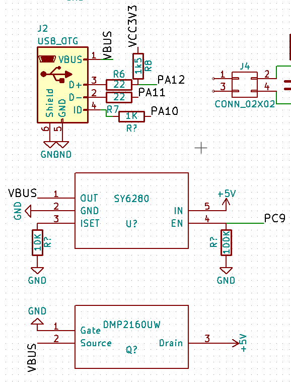
From the datasheet, the DMP2160UW pinout is:
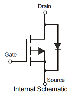
- DMP2160UW.png (11.81 KiB) Viewed 347 times
well, then now is the right time to turn it around XD
Here is a short TODO list:
- Add teardrops => Check https://github.com/svofski/kicad-teardrops
- Panelization => Check pcb-panelizer ( http://blog.thisisnotrocketscience.nl/p … panelizer/)
- Fix fill area minimum width => Fixed Top & Bottom GND zones minimum width to 6 mils
- Added some missing GND tracks between thermal pads due to previous change
- Problem with PCB edges in 3D view => Fixed by @racemaniac
- USB connector holes are too small => Fixed pads for J5 (micro USB) to be oval instead of round
- Remove Ref/Value for U3 (STM32) on PCB top => OK
- Option: Add an IMU somewhere on the bottom PCB size on an SPI or I2C bus to get a fully working flight controller board! i am thinking of an Invensense MPU6000 hooked to an SPI bus in order to get 8ksps performance
- Option: Add an RGB LED => 0603?
- Power AP2112 from +5V, not from +3.3V
- Add ferrite bead between GND and AGND
- Replace 32kHz crystal by smaller FC-12M, may be required for previous item
- Option: Add MCP73831 LiPo battery charger (would require an ideal diode like D3/FET2/R6 in the Olimexino ATMega32U4 schematics)
- Add pad/pin for VBUS for external PA9 VBUS_SENSE feature (USB Host) => Added a series resistor between VBUS and PA9 to avoid short-circuits
- Adjust solder mask clearance to 0
- Make VBAT trace thinner
- Provide footprint for parallel capacitor near SDCard and voltage regulators
- Fix MOSFET direction => replace by an SS12 Schottky diode
- Added PWR_FLAG to schematic to remove ERC warnings
- Replaced NC by real Kicad ones to remove ERC warnings
- Cleaned up Expansion connector labels in schematic
- Cleaned up traces for PA13-14 and PC13-15
- Changed micro USB connector to BSC-Elec U02-BFD3111B0-009
- Option: add an SPI Flash chip as an alternative to SDCard connector (overlapping footprints)
- Add optional shunt resistors to route a single bit SPI bus to the SDCard connector for devices without SDIO interface => NOT POSSIBLE, too tight!
All volunteers welcome!
i thought of it as a high side switch that is always on, and from what i can see the load (+5V in our case) would then be on its drain, as we originally drew. but that is not correct?
it drives me crazy when googling i can’t find clear answers for something as basic as this XD
[Squonk42 – Wed Dec 06, 2017 7:58 am] –
Please look at the Arduino Due schematic and TI AN above.
I can see the schematic, but i want to understand why it is so XD
Otherwise i’ll keep making the same mistake >_<
What is the purpose of the FET Q1
Which direction is it supposed to prevent. e.g. USB -> 5V pin , or 5V pin to USB
It definitely won’t stop 5V pin -> USB because of the internal diode as show in the symbol.
[Squonk42 – Wed Dec 06, 2017 9:02 am] –
Exactly, the idea is to allow USB to power the +5V, but not the opposite direction (we want to control VUSB using the SY6280 USB load switch), so the MOSFET body diode should be USB => +5V, like in the Arduino Due schematic and TI’s AN.
but since we’re also pulling the gate low, won’t it also conduct the other way around anyway?
Is it then maybe this that we want to create:
https://electronics.stackexchange.com/q … ransistors
but that’s then with 3 transistors >_<
I presume we are not simply using a diode on the 5V input, because you don’t want the 0.5V drop across the diode ?
AFIK the Maple mini just uses a diode for this.
What else uses the 5V input ? that really requires 5V, and not 3.3V from the regulator.
Even if the diode dropped 0.5V that would still be 4.5V on the input to the regulator, and I thought that would be enough voltage for some regulators to output 3.3V ??
It is working in TI’s AN only if you reverse the battery, and because there is only a load on the right side.
In the Arduino Due schematic, there is one that is polarized by a comparator circuit. How the MOSFET bottom circuit works is still a mystery.
Max current is 1A with the AP2114, and this may be used by external components in addition to the STM32F405 current consumption. But if we use a Schottky diode, the drop is only 0.3V, not 0.6V, so the max power dissipation is the diode is 0.6W. A 4mm x 2mm (vs. 3 mm x 2.5 mm for the MOSFET) diode such as an PMEG3010ER or MBRM130LT1G could handle that…
EDIT: well, maybe not: Taj is 220°C/W, so for 0.6W, this is a 132°C temperature rise… with a max Tj of 150°C, you blow the diode @1A above 18°C! It can only stand up to 0.5A @ 40°C.
If the drain voltage was equal to the gate (so drain shorted to gate, which is ground), the FET would stay closed, and the internal diode is reversed, so there is no current flowing to the short.
Just read thru TI note, so it’s for reverse current protection, not short circuit. I wonder why it needs that on the USC2 power source, is not like you can reverse a USB cable… But on the other hand, it also blocks current flowing from the load to the USB port, so that port can be used to power the board, but the board will not power something connected to that port.
Makes sense in the DUE since that’s not the native port. In our case since we can use the USB port as host and connect a slave, we don’t want that circuit or would prevent us from powering a slave.
Am I right?
[victor_pv – Wed Dec 06, 2017 2:42 pm] –
Perhaps the bottom FET is just short circuit protection?
If the drain voltage was equal to the gate (so drain shorted to gate, which is ground), the FET would stay closed, and the internal diode is reversed, so there is no current flowing to the short.Just read thru TI note, so it’s for reverse current protection, not short circuit. I wonder why it needs that on the USC2 power source, is not like you can reverse a USB cable… But on the other hand, it also blocks current flowing from the load to the USB port, so that port can be used to power the board, but the board will not power something connected to that port.
Makes sense in the DUE since that’s not the native port. In our case since we can use the USB port as host and connect a slave, we don’t want that circuit or would prevent us from powering a slave.
Am I right?
For a MOSFET to pass/block, what matters is the Vgs compared to its threshold value (negative for a P-type).
But you are probably right for the Due. In our case, we cannot use this solution, and I cannot find a single-component solution to implement this protection, except for a Schottky diode that will heat the birds!
[Squonk42 – Wed Dec 06, 2017 3:06 pm] –[victor_pv – Wed Dec 06, 2017 2:42 pm] –
Perhaps the bottom FET is just short circuit protection?
If the drain voltage was equal to the gate (so drain shorted to gate, which is ground), the FET would stay closed, and the internal diode is reversed, so there is no current flowing to the short.Just read thru TI note, so it’s for reverse current protection, not short circuit. I wonder why it needs that on the USC2 power source, is not like you can reverse a USB cable… But on the other hand, it also blocks current flowing from the load to the USB port, so that port can be used to power the board, but the board will not power something connected to that port.
Makes sense in the DUE since that’s not the native port. In our case since we can use the USB port as host and connect a slave, we don’t want that circuit or would prevent us from powering a slave.
Am I right?For a MOSFET to pass/block, what matters is the Vgs compared to its threshold value (negative for a P-type).
But you are probably right for the Due. In our case, we cannot use this solution, and I cannot find a single-component solution to implement this protection, except for a Schottky diode that will heat the birds!
Maybe a diode like this: https://www.vishay.com/docs/88746/ss12.pdf
(also easily & cheaply found on aliexpress)
or a bit bigger & certainly capable of 1A: https://www.vishay.com/docs/88712/s2a.pdf
When Luke first posted here about the SY6280 I read thru a bunch of other USB protection ICs, but I can’t remember is any allowed current to flow back in some condition.
I’m trying to understand, so correct me if I’m wrong, but we want to achieve this:
-Power the board from USB.
-Power a slave device from the board usb
-Prevent current flowing back to the USB port if the USB has some voltage, but the board +5 voltage is higher.
Something like this, but single component:
http://www.linear.com/product/LTC4160
Actually reading thru that, is achieves multiple functions. Current limiter, battery charger, and switching regulator. Perhaps is worth it since it would replace multiple components.
[racemaniac – Wed Dec 06, 2017 3:11 pm] –
Maybe a diode like this: https://www.vishay.com/docs/88746/ss12.pdf
(also easily & cheaply found on aliexpress)
or a bit bigger & certainly capable of 1A: https://www.vishay.com/docs/88712/s2a.pdf
The first one has a Vf of 0.5V and is already 4 mm x 2.54 mm but may be acceptable with Tja of 88°C/W (44°C rise), the second has Vf of 1.15V and is even larger, so no way.
The MAX40200 ideal diode would match perfectly, but it is not cheap and cannot be found on Aliexpress:
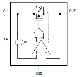
- MAX40200.png (10.37 KiB) Viewed 134 times
This is another one, a bit cheaper than the Linear one:
http://www.ti.com/lit/ds/symlink/bq24296.pdf
Can do power management + battery charging, and works with USB OTG, but cheapest cost seems around $1, and still needs a few external components.
[victor_pv – Wed Dec 06, 2017 3:12 pm] –
Something like this, but single component:
http://www.linear.com/product/LTC4160Actually reading thru that, is achieves multiple functions. Current limiter, battery charger, and switching regulator. Perhaps is worth it since it would replace multiple components.
This component is $0.30 on Taobao, plus power inductor, MOSFET and other components: probably too expensive and too large. All PMIC will have the same problems.
I am trying to understand how FET2 works in this schematic:
https://www.olimex.com/Products/Duino/A … rev_A3.pdf
[Squonk42 – Wed Dec 06, 2017 3:29 pm] –[racemaniac – Wed Dec 06, 2017 3:11 pm] –
Maybe a diode like this: https://www.vishay.com/docs/88746/ss12.pdf
(also easily & cheaply found on aliexpress)
or a bit bigger & certainly capable of 1A: https://www.vishay.com/docs/88712/s2a.pdfThe first one has a Vf of 0.5V and is already 4 mm x 2.54 mm but may be acceptable with Tja of 88°C/W (44°C rise), the second has Vf of 1.15V and is even larger, so no way.
The MAX40200 ideal diode would match perfectly, but it is not cheap and cannot be found on Aliexpress:
MAX40200.png
Indeed, the bigger ones are too much, but those SS12 diodes may be an option? and they’re indeed big, but if we can get some traces between its pads, it might work out? And it’s also a cheap & easy to find diode, so ideal for the kind of board we’re making.
[Squonk42 – Wed Dec 06, 2017 3:45 pm] –
I am trying to understand how FET2 works in this schematic:
https://www.olimex.com/Products/Duino/A … rev_A3.pdf
Seems like this circuit, this has the explanation on how it works. Called Q1 here:
https://behindthesciences.com/electroni … y-circuit/
The FET is basically just acting like a diode ( if it’s connected correctly ), and will handle the expected current.
But the issue is that sometimes the battery is allowed to feed the USB for OTG operation.
So can we connect the gate to a GPIO, and require software control for then using the battery connection ?
Possibly not, as for some time during startup the GPIO may not be the correct value?
Or alternatively, just directly connect VBAT , and users need to use their brains and not connect USB and battery at the same time. perhaps make the track very thin, to act like a fuse, so if the user does this, it burn the track but not the board..
Or use a jump link.
Looking on AliExpress there seems to be multiple vendors
Its 1A 20V
Edit.
I am changing my copy of the schematic now.
I’ve had to include the diodes library, but I guess now its in the schematic, I need to move the symbol into the board’s custom lib.
I don’t normally bother on components like diodes etc which are common, and only use custom libs for parts not available in KiCads default libs, but I can to manually add it to the boards on library, if we are happy with that diode
Edit.
Its a bit of a pain to do, but I’ve added a 1N5817 to the BluePill lib (in my local copy)
The diode prevents the +5V pin feeding the USB VBus
SS12 diodes are extremely common, even on Aliexpress:
https://www.aliexpress.com/item/sku/32830718059.html
However I don’t know what package the SS12 uses
SS12 are extremely standard SMD power diodes, they use an “SMA” (also called “DO-214AC”) package, plenty of them on Digi-Key:
https://www.digikey.com/products/en/dis … 280?k=ss12
AFAICT, it corresponds to the “D_SMA” footprint in the “Diodes_SMD” footprint library in Kicad. But in general I prefer to use my old trusted footprints rather than using an existing one that I have not checked against the real thing. One thing that makes me suspect problems is the “D_SMA_Handsoldering” variant…
I’ll change the name of the library symbol from 1N5812 to SS12 (its the same visual symbol) , and use the D_SMA footprint
[Squonk42 – Thu Dec 07, 2017 9:35 pm] –
AFAICT, it corresponds to the “D_SMA” footprint in the “Diodes_SMD” footprint library in Kicad. But in general I prefer to use my old trusted footprints rather than using an existing one that I have not checked against the real thing. One thing that makes me suspect problems is the “D_SMA_Handsoldering” variant…
KiCad has a lot of handsoldering variants for smd components. I assume it’s just some bigger pads so you can more easily solder them with your soldering iron. I always use the regular pads as i use solder paste & stencil (and since space is tight XD)
I presumed the same thing about “hand soldering” versions, but never took the time to look
I do recall selecting them sometimes when I know the board is actually going to be hand soldered, i.e I did some boards for a small company and they didnt have their SMD reflow setup to start with, so as there was plenty of room on the PCB they wanted everything to be big SMD e.g. 1206 sizes for R and C and LEDs, so that they could be hand soldered.
[RogerClark – Thu Dec 07, 2017 9:53 pm] –
@racemanicI presumed the same thing about “hand soldering” versions, but never took the time to look
I do recall selecting them sometimes when I know the board is actually going to be hand soldered, i.e I did some boards for a small company and they didnt have their SMD reflow setup to start with, so as there was plenty of room on the PCB they wanted everything to be big SMD e.g. 1206 sizes for R and C and LEDs, so that they could be hand soldered.
just did a quick check with the SMA diode footprint: it’s indeed pads that extend beyond the diode so it can easily be soldered with an iron.
Of course, these PCBs have the +3.3V voltage problem on the Analog LDO input, and the MOSFET problem too ![]()
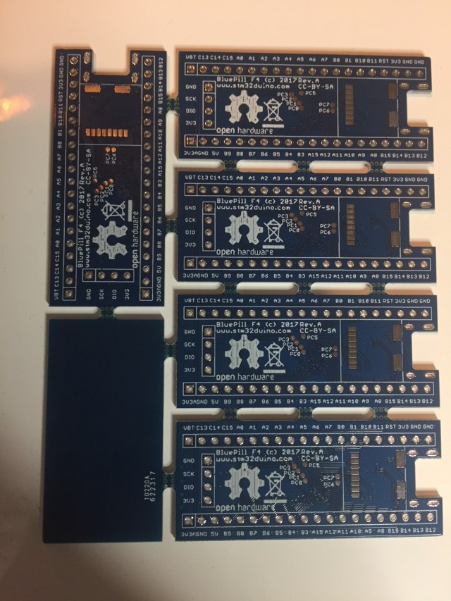
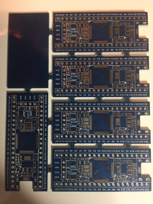
About the hand soldering versions, I compared them to the normal component for several components, and the pads extend more in the outside. I guess the purpose is so a thin soldering tip can touch the pad. I did replace one diode that blew up in a maple mini clone without an issue, and the pads most definitely were just normal size, and my iron tip is not pencil sharp either. Normally the diode terminals seems to always extend up the part (at least the few smd models I have hand soldered), so the soldering iron can touch and heat the terminal, and transfer heat from the there to the PCB pad.
If the intention is to make them easy to hand solder, I think using the hand solder version of the footprint would be a good idea, but if we are just making a few of them for prototyping until we are happy, and we all feel confortable with hand solder/skillet/reflow, then better use the real version of the pads that would would send to a factory, so no last minute mistakes because we replace a hand solder version for a normal solder version later on.
One more thing, why is the SY6280 in to +5V and out to VBUS? in that configuration, the board can power the USB, but the USB can’t power the board. Did I miss something? Ok I see the SY6280 is not provided to power the board, but to power the USB port,controlled by PC9.
The consensus was just to use a Schottky diode, so I was updating my copy of the files, but so far I’ve only had time to update the schematic, and I need to rename the schematic symbol to a SS12 as I didnt see a SS12 in the kicad diodes lib (but I will double check)
I’ve not looked at the PCB yet, but it should be OK as it replaces the 3 pads on the fet, with 2 pads
I had to move one resistor a bit, and move a few tracks.
Hopefully what I’ve done is OK, but if not we can revert to the previous version.
BTW There is now more space near the diode, so we may be able to move other things to this space
I didnt change anything else, though I noticed some of the tracks could be cleaned up a bit, as they seemed to have unnecessary small kinks in them.
Please download it and let me know if I’ve stuffed up or not ![]()
PS. DRC seems OK (no errors) and I looked in the 3D viewer and there seemed to be enough space between the diode and the regulator
[victor_pv – Fri Dec 08, 2017 2:01 am] –
I just found the perfect component for the job, MAX40200, but is not worth it, can’t find it in aliexpress, and in mourser costs $0.5.
I mentioned it in a previous post, but it is too exotic and expensive.
And we don’t have the room to fit the additional dual transistor and 2 more resistors to have a current mirror like the RPi, so either we put an Ss12 Schottky diode or we put nothing like the origial Bluepill.
I will check Roger’s additions.
Regarding the track clean up, this may be intentional in order to accomodate for the teardrops (smooth junction between track and pad to remove stress caused by etchint sharp corners), I had to turn some segments to pass DRC. But of course, it may happen that I forgot to optimize some tracks too!
For the teardrops, you have to duplicate the PCB just before generating the gerber files and run an automatic script that will add them with no way back, then panelize the result, hopefully with the tool found by @racemaniac to get the result above (this was in EagleCAD).
I moved R1 a bit, but in hindsight, I can now move it back to the left a bit.
I initially tried to have D3 closer to the regulator and needed to move R1 but looking in the 3D view they looked unnecessarily close
So I moved the track from PA11 to USB DM, to allow D3 to move even further away from the regulator if necessary.
I also moved the tracks and vias on PB12 and PB13 to make more room for D3
PA11 and P12 tracks can be moved down even more as could PB12 and PB13 if we needed space next to D3 for anything else
Arggghh.
I just noticed a stub of the 3.3V track, sticking out. I’ll remove it …
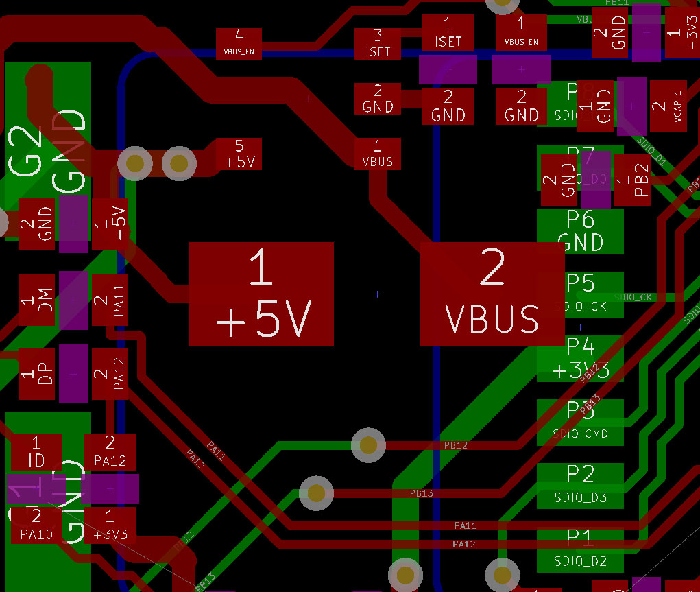
- diode.jpg (198.16 KiB) Viewed 151 times
OK.
I’ll need to check why that track is there. I didnt add it and I can’t see what it would have been connecting to
Edit
I checked and I’ve somehow lost 5V pad which was at the end of that track.
I’ll reinstate the track and that pad
BTW.
I can’t see why VCAP1 and PB2 tracks are routing around something, which I can’t see
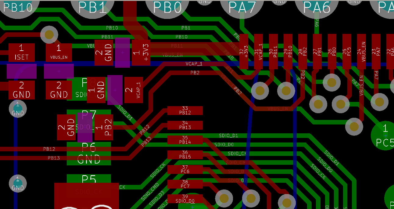
- VCAP1_PB2.png (47.93 KiB) Viewed 141 times
I’ve removed U1 not Q1
Apologies
I’ll try to fix it now
[RogerClark – Fri Dec 08, 2017 10:08 am] –
I screwed up big timeI’ve removed U1 not Q1
Apologies
I’ll try to fix it now
lol, that happens ![]()
it’s great to see us working together towards this ![]() . i was hoping someone else would pick up the pcb development, so this weekend i can focus on writing software for my saber boards
. i was hoping someone else would pick up the pcb development, so this weekend i can focus on writing software for my saber boards ![]()
i’ve got multiple simultaneous files streaming from an sd card working pretty well ![]() (still some last bugs/details to finish, and somewhere in the future do yet another rewrite as i’m now finally coming close to an API i like, and a feature set that makes sense for what i’m trying to do
(still some last bugs/details to finish, and somewhere in the future do yet another rewrite as i’m now finally coming close to an API i like, and a feature set that makes sense for what i’m trying to do ![]() ).
).
got my board playing 4 48khz stereo wavs from the sd card, and mixing them together ![]() .
.
I should have some time this WE to browse through the TODO list.
I’ve reverted back to before I started
I’m going to need to move a lot of components
I think I’ll need to move the group of components (R’s and C’s etc) next to pins for B11,B10,B1 to the right

- move_components.png (49.25 KiB) Viewed 235 times
Or do we need a 1A diode. Will a 500mA one do ?
If I push U4 and a load of the components next to it, to the right, there isnt really enough room, and one of the resistors has to be moved completely out the way, and at the moment I can’t see a good place for it.
And its getting too late for me to do any more today.
So I suspect you guys will have it done before I wake up tomorrow ![]()
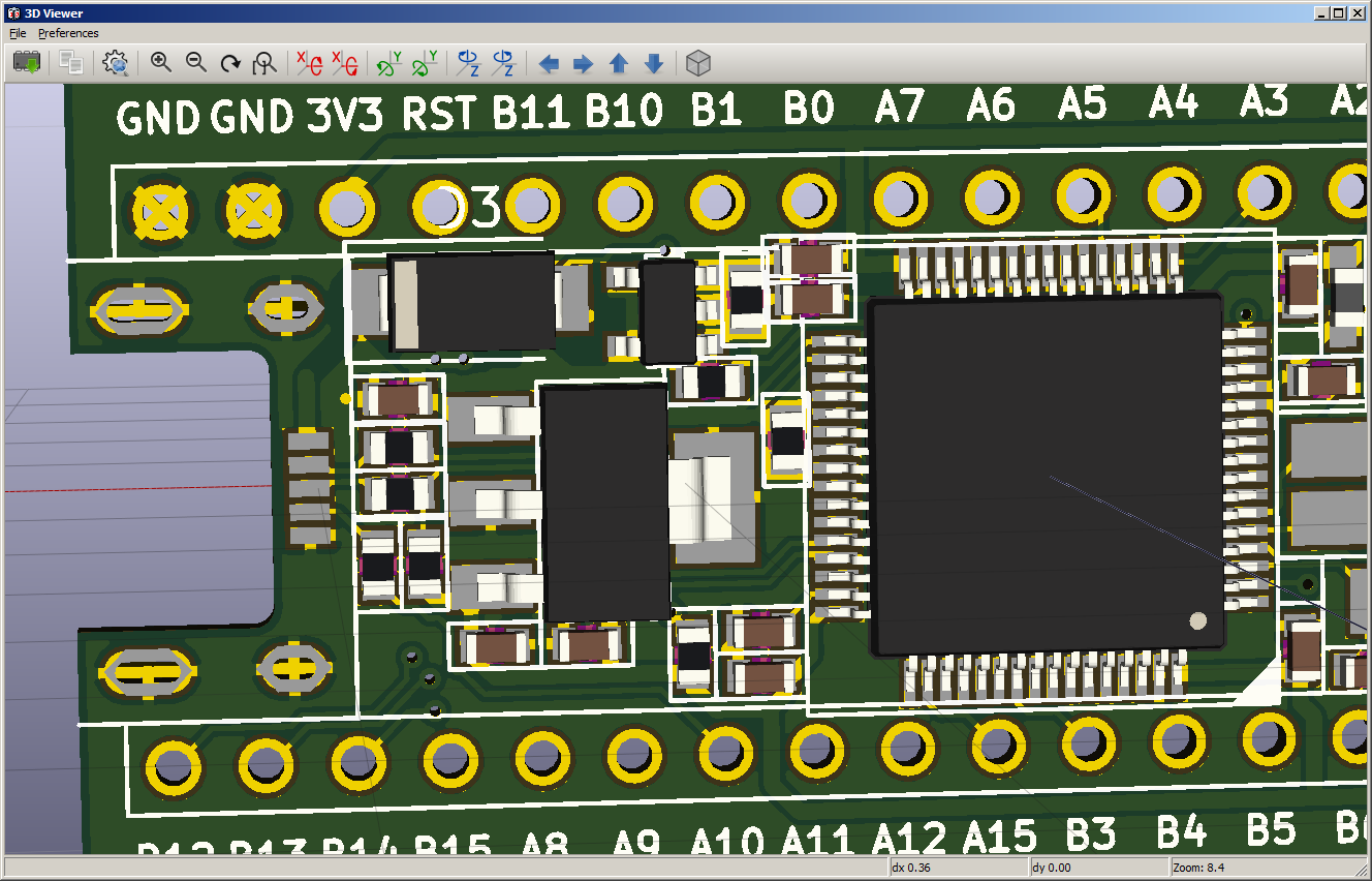
- add_SS12_diode.png (107.92 KiB) Viewed 233 times
[RogerClark – Fri Dec 08, 2017 11:17 am] –
Can we get the same spec diode in a smaller package, as is a real squeeze getting the it to fitOr do we need a 1A diode. Will a 500mA one do ?
This is questionable! We chose the main LDO to be able to deliver 1A, as the STM32F405 already sinks 450 mA max itself; we added some room to power external components as well (SDIO…).
However, the USB 2.0 spec only allows delivering 500 mA, and this is even conditioned by a proper negotiation beforehand, otherwise, it is limited to 100 mA. Despite this limitation, there are a lot of wall adapters with an USB A socket that can deliver more than that, and it is easy to find a USB A to micro USB B cable to power the board over the micro USB B socket.
There are some smaller 1A Schottky diodes, but they are not as common and rather expensive: https://toshiba.semicon-storage.com/inf … e=CUS10S30
So, do we limit the power supply from the USB to 500 mA? If yes, this one may be interesting:
http://www.onsemi.com/pub/Collateral/MBR0520LT1-D.PDF
https://www.aliexpress.com/item/sku/1985290956.html
[Squonk42 – Fri Dec 08, 2017 12:55 pm] –[RogerClark – Fri Dec 08, 2017 11:17 am] –
Can we get the same spec diode in a smaller package, as is a real squeeze getting the it to fitOr do we need a 1A diode. Will a 500mA one do ?
This is questionable! We chose the main LDO to be able to deliver 1A, as the STM32F405 already sinks 450 mA max itself; we added some room to power external components as well (SDIO…).
However, the USB 2.0 spec only allows delivering 500 mA, and this is even conditioned by a proper negotiation beforehand, otherwise, it is limited to 100 mA. Despite this limitation, there are a lot of wall adapters with an USB A socket that can deliver more than that, and it is easy to find a USB A to micro USB B cable to power the board over the micro USB B socket.
There are some smaller 1A Schottky diodes, but they are not as common and rather expensive: https://toshiba.semicon-storage.com/inf … e=CUS10S30
So, do we limit the power supply from the USB to 500 mA? If yes, this one may be interesting:
http://www.onsemi.com/pub/Collateral/MBR0520LT1-D.PDF
https://www.aliexpress.com/item/sku/1985290956.html
how about this one:
https://www.aliexpress.com/item/100PCS- … eLevelAB=0
http://www.mouser.com/ds/2/258/B5817W-B … 276623.pdf
Same package as the 0.5A you’re mentioning, but also 1A (and bit lower votlage drop)
[racemaniac – Fri Dec 08, 2017 1:35 pm] – how about this one:
https://www.aliexpress.com/item/100PCS- … eLevelAB=0
http://www.mouser.com/ds/2/258/B5817W-B … 276623.pdfSame package as the 0.5A you’re mentioning, but also 1A (and bit lower votlage drop)
There is something I don’t understand in the datasheet: max dissipation is 250mW, however Vf is max 0.45V x 1A = 450mW to dissipate.. Tj 25°C !?!
[Squonk42 – Fri Dec 08, 2017 1:48 pm] –[racemaniac – Fri Dec 08, 2017 1:35 pm] – how about this one:
https://www.aliexpress.com/item/100PCS- … eLevelAB=0
http://www.mouser.com/ds/2/258/B5817W-B … 276623.pdfSame package as the 0.5A you’re mentioning, but also 1A (and bit lower votlage drop)
There is something I don’t understand in the datasheet: max dissipation is 250mW, however Vf is max 0.45V x 1A = 450mW to dissipate.. Tj 25°C !?!
hmm, indeed pretty strange >_<
also don’t get it O_o
https://www.aliexpress.com/wholesale?ca … xt=LTC4357
https://www.diodes.com/assets/Datasheets/ds30217.pdf
https://www.aliexpress.com/item/sku/32841683463.html
I am not sure why this diode is so much bigger than the FET it replaced.
I know that the FET was in the circuit the wrong way around, but is there no way to get a FET to behave like this diode ?
( to achieve the same functionality in a smaller package)
[RogerClark – Fri Dec 08, 2017 8:04 pm] –
I think it can be made to fit, but virtually all the other components between the USB connector and the MCU probably need to be moved, and a load of tracks rerouted.I am not sure why this diode is so much bigger than the FET it replaced.
I know that the FET was in the circuit the wrong way around, but is there no way to get a FET to behave like this diode ?
( to achieve the same functionality in a smaller package)
because the diode has a voltage drop that is WAY higher than the fet ![]() . it has to dissipate way more heat, so it’s bigger…
. it has to dissipate way more heat, so it’s bigger…
We must respect the component courtyards: for example it is forbidden to put components in the corner of the STM32 as some pick&place machine may grab the chip by the corners or use a suction cup on the top. And the U1 (LDO) needs the largest possible copper area below it in order to dissipate the heat. It will be thus difficult to move much of the components around.
The diode is bigger because it needs to dissipate more heat: when there is current (up to 1A) flowing in the non-blocking direction, a Schottky (metal-silicon junction) diode has a forward voltage (Vf) ranging from 0.2-0.3 to 0.5V (vs. 0.6V for an NP silicon diode), resulting in a power of 1A x 0.6V = 0.6W to dissipate in heat. Then, the thermal resistance of the package (in °C/W, the smallest package, the highest resistance value) then gives you what will be the increase in temperature for this power, that you need to add to the ambient temperature to get junction temperature, which must never exceed a maximum value (generally 150°C).
Unlike the diode, a MOSFET when unblocked will feature a drain/source resistance (Rdson) of a few tens of milliohms (75 to 160 mhoms for the DMP2160UW-7), resulting in a power of 0.160 mohms x 1A x 1A = 0.16W, almost 4x less, so the package can be much smaller for a FET.
The MOSFET was not only the wrong way around to let current flow from Vusb to +5V, but it was actually always on, whatever the current direction. Mounting a MOSFET with its gate connected to ground is only useful to prevent a reverse battery connection to a circuit only sinking current, NOT to replace a diode between 2 voltage supplies like we did.
For the MOSFET to be used as an “ideal diode” (because of its low voltage drop of 0.16 mohms x 1A = 0.16V), the gate must be controlled by a circuit that will depend on the relative polarity on both sides of the diode. It can be achieved using an op amp like in the Arduino Due (see IC1B in the Arduino Due schematic), a current mirror like in the RPi B+, or using an exotic and rather expensive MAX40200 ideal diode integrating the MOSFET and the comparator.
Is this just to keep it 100% compatible with the BluePill ?
Is it just protection if someone powers via 5V and connects USB?
I think this may just have to be a limitation, that it’s not practical to have the protection diode on the board, as there is simply not enough space.
One other alternative could be 2 x 0.5A diodes, as perhaps they is space for 2 smaller diodes in different locations.
However my vote would be not to have the diode at all
[RogerClark – Fri Dec 08, 2017 9:16 pm] –
Is it really such a major problem if 5V is connected directly from the USB to that pin?Is this just to keep it 100% compatible with the BluePill ?
Is it just protection if someone powers via 5V and connects USB?
I think this may just have to be a limitation, that it’s not practical to have the protection diode on the board, as there is simply not enough space.
One other alternative could be 2 x 0.5A diodes, as perhaps they is space for 2 smaller diodes in different locations.
However my vote would be not to have the diode at all
if we ditch the diode, we also ditch the other other current limiter, and then the issue is that as usb host you can’t accept a powered device. That is a tradeoff we can choose for, but it’s a limitation (but would indeed save us a TON of boardspace)
If people really like the board and think its worth the extra money for the expensive MAX40200, then it would not be that hard to produce boards with that on it.
But for now, I think we need to move forward..
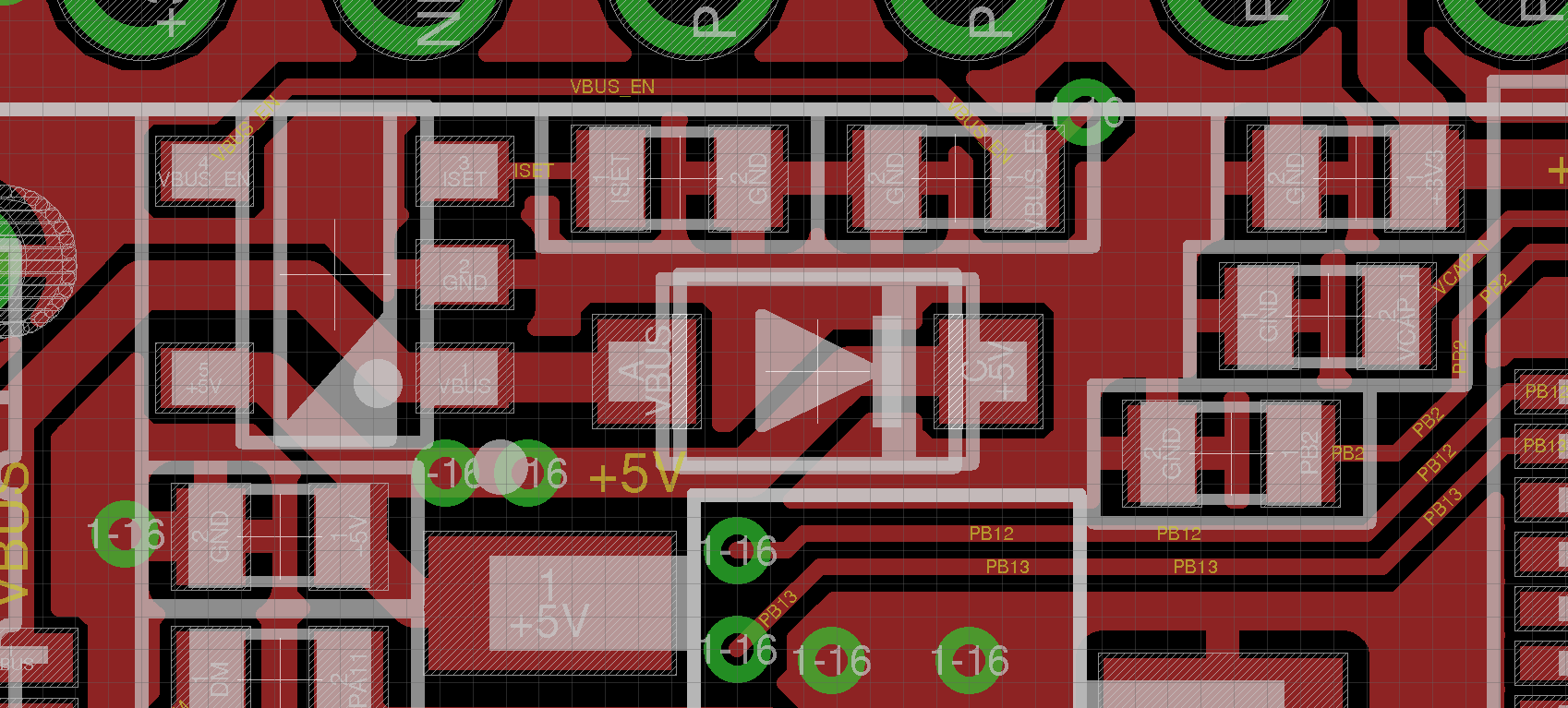
- 1N5819HW.png (119.29 KiB) Viewed 149 times
Here is what KiCad is showing for the regulator U4 and the diode
- D_SMA_footprint.png (7.06 KiB) Viewed 146 times
1N5819HW is also a 1A Shottky diode able to withstand the required power and is easy to find on Aliexpress:
https://www.diodes.com/assets/Datasheets/ds30217.pdf
OK.
A smaller package can probably me made to fit.
And I am pretty confident that if I replace the 32kHz crystal by a smaller FC-12M package as suggested by @racemaniac, I will be able to fit the ferrite bead between GND and AGND, which should cover most of the problems we found so far.
Then, we have all the options as footprints only (battery charger, IMU, RGB LED…)!
Just in case I’m missing something with KiCad.
Can you guys confirm that the footprint dragging doesnt work in OpenGL mode, but the interactive Push / Shove (of tracks) feature only works in OpenGL mode.
So if i want drag a track I need to switch to OpenGL to take advantage of the Push/Shove but if I want to drag a component and keep the track segments attached by simple rubber banding, this only works in “Canvas” view mode ??
PS. I’m using the latest stable version (4.0.7) not the “nightly” builds (I’ve heard that the nightly’s are much more advanced than the stable, but normally the Stable is good enough for me)
I haven’t tried dragging a component in canvas mode, need to try that, but in OpenGL dragging a component doesn’t drag the tracks attached to for me.
So openGL mode is the same for me as you describe.
Thanks.
Hopefully in the next version they will unify things, as its not ideal having to switch in and out of OpenGL mode
This means that for reliable operation, the bootloader should have stable levels on USART1_RX (PA10), USART3_RX (PB11 and PC11), CAN2_RX (PB5) pins during boot, in addition to BOOT0 being high and BOOT1 (PB2 pin) being low, which is the case when the BOOT0/USER button is pressed.
This is confirmed by a remark in the MicroPython board schematic:USB DFU requires stable levels on PA10, PB5, PB11 & PC11. PB2 must be low during boot.
Even if the pins were randomly toggling with noise it would only be a 1 in 256 times that the data would match the pattern.
And in reality I don’t think the input pins randomly toggle, unless you attach a long length of wire to them to pickup noise, and in most cases that would pick up mains hum of 50 or 60 Hz
e.g.
With the RobotDyn Black Pill boards that I received the other day, they did not send jump links, so I did not solder the boot0 or boot1 pins. I just flashed the bootloader via STLink and they worked fine even with boot0 technically floating.
The Maple mini does not pull boot1 low but unless you stick your finger on that pin, it’s possible to reflash just by pulling boot0 high.
I need to test this hypothesis, but I suspect the pins have a tendency to float low.
That said, I see we have two options:
- add extra components to pull those pins low, which may affect their usage for other functions (if the pull down is too weak, it may not have an an effect other than if the pins are floating, if the pull down is strong, then it may affect other uses.
- leave then like they are, in the particular conditions they may affect usb dfu bootloader
My vote goes for the second option, since I believe the conditions in which may cause the bootloader to not get to the USB port, would be only if there is something in serial sending that character, and in that case the pull downs would not help, since I would expect whatever serial device is in the other end to be stronger than the pull downs, otherwise your serial functionality is compromised. I don’t think something else other than serial will cause it to randomly get the special character.
If it happens, then the stlink pins are available, and if not, we can load our own bootloader that goes straight to USB and that’s it. There is code from STM that Roger and me tested a couple of months back. If we need to, we can work on that to make it funtions the way we want. We could even add sdio support to upload boards with a bin in the sdcard.
I will then implement solution #2 (not care about it) since 1) I think this situation is unlikely and can be fixed by a simple retry and 2) it is easier, since there is nothing to do!
Uploading a board from a bin file on the sdcard would be great!
I fixed all problems in the TODO list, it just needs more cleanup (more trace shufflîng, 3D models for new 32kHz crystal and Schottky diode, etc.).
I checked the board and it does not have a pulldown on PA9 or PA10
I also checked the STM32 Stamp schematic (there is a copy in my repo in the STM32F4Stamp folder) and that board does not have a pulldown on PA9 or PA10 (it can however use PA10 to connect to the serial port, I presume to signal OTG) if a jump link is installed
I think the micropython team are being over-cautious.
BTW. I find using the built in DFU hard to use, as its unclear whether code can reboot/reset the MCU into its internal DFU mode, so you would have to keep boot0 high, and press the reset button each time
(It may be possible to jump to the bootloader but I don’t think anyone has proved they can do that)
I know Victor has written a DFU bootloader, based on STM’s example code, and they would initially be the best thing to use (apart from STLink)
However because both the internal DFU bootloader and the one from ST’M’s code, use DFUSe, it is not compatible with the F103 DFU drivers or DFU-Util, so if I get time I want to investigate porting the existing F1 bootloader to F4
I know its possible, but the code to do it seems to have been lost.
[RogerClark – Mon Dec 11, 2017 6:32 am] –
I’ve tested DFU upload on one F4 board, and it seemed to work every time.I checked the board and it does not have a pulldown on PA9 or PA10
I also checked the STM32 Stamp schematic (there is a copy in my repo in the STM32F4Stamp folder) and that board does not have a pulldown on PA9 or PA10 (it can however use PA10 to connect to the serial port, I presume to signal OTG) if a jump link is installed
I think the micropython team are being over-cautious.
BTW. I find using the built in DFU hard to use, as its unclear whether code can reboot/reset the MCU into its internal DFU mode, so you would have to keep boot0 high, and press the reset button each time
(It may be possible to jump to the bootloader but I don’t think anyone has proved they can do that)
I know Victor has written a DFU bootloader, based on STM’s example code, and they would initially be the best thing to use (apart from STLink)
However because both the internal DFU bootloader and the one from ST’M’s code, use DFUSe, it is not compatible with the F103 DFU drivers or DFU-Util, so if I get time I want to investigate porting the existing F1 bootloader to F4
I know its possible, but the code to do it seems to have been lost.
OK, thank you Roger for testing, I also think that this is over-engineering.
In AN2606, Table 3, there is a memory location, maybe it is just a matter of jumping there?
Yes. I think in theory it can be done. But I”ve read various posts on various forums where people seem to be having trouble doing that
https://www.youtube.com/watch?v=cvKC-4tCRgw
Seems to be straightforward, have not tested it thought, but should be easy to test. I’ll try when I get a second.
@Roger you are giving me too much credit, I barely modified a few things. It’s mostly the code from STM, which Chriss Bar had already taken and done a few modifications.
I am sure we can modify it to be 100% compatible with our bootloader, alt modes and all. But if we can reliably use the hardware one, then no need for it and saves a few KB of flash, and the same BIN would be valid no matter what method is used for upload (serial, dfu, stlink…)
Re: F4 DFU bootloader
You managed to get it working more than I did ![]()
Re: Using the old bootloader. From the code snippets I’ve seen, I don’t think that too many changes are needed to get the old bootloader to work on the F4 and like you say, its smaller and can use all the existing binaries and drivers.
So perhaps if I get time over Christmas I’ll setup system workbench, or True Studio etc, and see if I can port it.
I think the register addresses for the GPIO are different (and also for the USB controls), and I know the GPIO clock settings etc will be different.
But the GPIO stuff should be easy to crib from the LibMaple F4 core.
The USB code in the LibMaple F4 code is a lot different from the F1, but I don’t know if there is a good reason for this.
Anyway, getting the bootloader LED flashing on the F4 would a be a good start !
[RogerClark – Tue Dec 12, 2017 4:36 am] –I think the register addresses for the GPIO are different (and also for the USB controls), and I know the GPIO clock settings etc will be different.
But the GPIO stuff should be easy to crib from the LibMaple F4 core.
I believe you are right about GPIO, just the base addresses are different, but same registers and flags in the same offsets, so should work just changing the base address.
Not sure about USB, haven’t looked, but flash is different too, larger pages and a mix of smaller and larger pages in the same device, but for writing to the flash perhaps you can reuse the parts from the STM code.
I had not considered the flash writing part of the code. It’s strange that the flash page size changes depending on where the flash page is.
On the F103 the page size is bigger on the devices with more flash, I remember looking into this, but can’t remember whether it was for the bootloader or the core.
https://github.com/victorpv/F4Bootloade … fu_flash.h
Its something like 1k on the Low Density MCU’s and 2k on the medium and possibly 4k on the High density.
But all pages in the same MCU will be the same size.
Having different sizes at different locations in the flash is a pain, as it would make the code a bit larger as it needs a case or if statement to handle it , in several places
So I’d probably need to look elsewhere for savings in code size, as it only just sits in 8k at the moment
i’m curious to see the new version
I am redoing it in Kicad, but I am much slower as I don’t know the software well enough, but I am still learning ![]()
Right now I have the symbols, footprint and 3D models for the FC-12M 32 kHz crystal and the SOD-123 diode, I routed the diode, but still need to apply the other remaining changes.
I am doing it on my spare time, not easy before X-Mas!
i was just curious to see the current iteration
However, it perfectly matches the one on the original Bluepill! I asked the vendor for a drawing, and will modify the footprint to be compatible with both.
I will share the Kicad files are soon as they are stable enough (hopefully before the end of this WE), before adding any option.
I eventually found a drawing that is a bitmap capture of the datasheet (I am still interested in it):
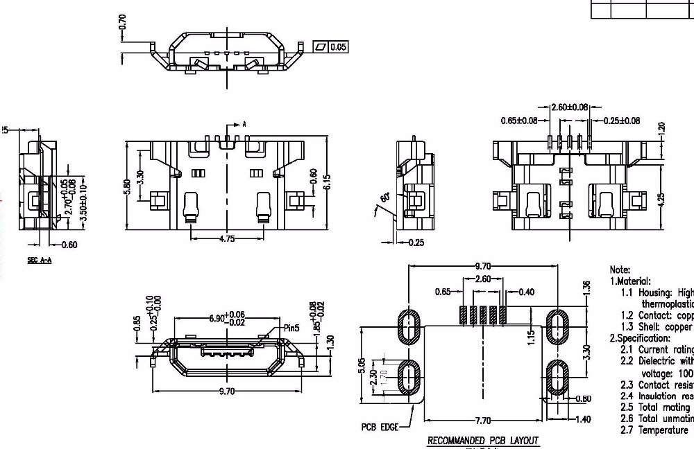
- image.jpeg (138.84 KiB) Viewed 214 times
If you are going to enlarge the front holes, may be worth enlarging the rear ones too a little bit just in case…
The main difference I see is that the front to rear holes separation is almost 1mm bigger in the molex ones, right?
EDIT: This one shows a lightly different design but the footprint seems to match with the one you posted:
https://www.aliexpress.com/item/50pcs-M … 19250.html
[Squonk42 – Thu Dec 14, 2017 2:41 pm] –
I think it is possible to design a single footprint that will work with all of them: the 5 USB pins have a standard pitch (but their footprint length may be 1.10 or 1.15 mm), there may be a “lip” at the front or it can be flat like for the Chinese ones, the biggest differences are regarding the legs, but by designing large and long enough oval holes, I am pretty confident we can accommodate a lot of different “harpoon” style models.
XD
exactly what i was thinking (but didn’t want to give you even more work XD)
BTW. I noticed that Eagle are now advertising it now supports Push And Shove routing, but KiCad has had that for ages ( in OpenGL disolay mode)
I also happened to notice a video by Dave ( EEVBlog) about how Autodesk have consistently changed what they said they would do in terms of licensing and prices, since buying Eagle, and their prices and licensing model seem to get worse every day.
What clinched it for me, was finding I can’t use the version of Eagle which I upgraded to, without signing in to Autodesk to use it, despite paying for a perpetual license for the previous version.
If I had realised the “update” removed its ability to operate without signing in, I would never have updated.So I now have a non functional copy of Eagle installed, and would have to find my original installer file, and remove the new copy and reinstall the old copy etc etc. which is never worth the time and effort.
I started to migrate away from Eagle, as soon as Autodesk bought it, so don’t have any recent boards designed using it.
And for my older boards, they were never very complex and I would take the opportunity to do them again from scratch in KiCad, and fix the problems most of them have e.g. replace component footprints with more readily available parts
Made one with each powersupply option so i could have a test how they work.
When i have some time i’ll assemble one, and give them a try ![]() .
.
As the noise on the ADC is one of the things we want to get better than the existing bluepills, does anybody have ideas of good testcases?
[racemaniac – Fri Dec 15, 2017 1:15 pm] –
As the noise on the ADC is one of the things we want to get better than the existing bluepills, does anybody have ideas of good testcases?
Pigoscope may be good code to visualize the noise. See what shows when floating, and when connected to known value with large resistors.
Since at the same time it reads ADC with DMA it may be using serialUSB or the SPI ports it may be getting some noise generated in the same board.
Here is a list of their micro USB connectors: https://bsc-elec.en.alibaba.com/product … ector.html
The one that is perfectly matching the Bluepill one is their model 008 (please notice the shell shape around the 5 USB pins):
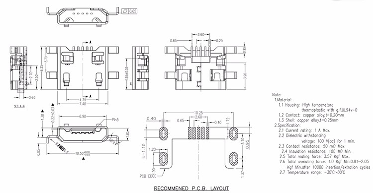
- BSC008.jpg (70.93 KiB) Viewed 255 times
[victor_pv – Fri Dec 15, 2017 1:45 pm] –[racemaniac – Fri Dec 15, 2017 1:15 pm] –
As the noise on the ADC is one of the things we want to get better than the existing bluepills, does anybody have ideas of good testcases?Pigoscope may be good code to visualize the noise. See what shows when floating, and when connected to known value with large resistors.
Since at the same time it reads ADC with DMA it may be using serialUSB or the SPI ports it may be getting some noise generated in the same board.
Anyone up for documenting how & what to test, and to do a testrun on the bluepill? (and to figure out how we can get a similar test running on the F4, or would the pigoscope code be compatible?)
There was an initial version without DMA, that for the purposes of measuring the adc noise should still work, and may run straight in an F4.
The current one may work in F3 MCUs though, since they are so close to the F1, or may work with just slight modifications.
What MCUs are you guys planning to put in these boards? just F405 and F411?
[victor_pv – Sun Dec 17, 2017 3:11 pm] –
I think you are right Roger. Perhaps with a few modifications it can work though.There was an initial version without DMA, that for the purposes of measuring the adc noise should still work, and may run straight in an F4.
The current one may work in F3 MCUs though, since they are so close to the F1, or may work with just slight modifications.
What MCUs are you guys planning to put in these boards? just F405 and F411?
just f405 atm
The 3D model for the micro USB connector is still the old Molex one, but the footprint is the one for the BSC Model 010 above (the one I bought from Aliexpress). If there are 3D modeler experts, I can provide the datasheet ![]()
Please let me know if you spot some errors! I tried my best not to break things, but who knows…
I merged the PR
[RogerClark – Sun Dec 17, 2017 9:05 pm] –
i think the option of using something like a F103RE or F103RG etc would be interesting as all the F1 core would work, plus it has DAC and SDIO, and this board would have better ADC noise performance
great idea ![]()
why didn’t i think of that XD
I thought the F103RB was just like a F103CB in a different package, so it has more pins
It does not have extra features like DAC and SDIO
But it would run the Pig-O-Scope firmware
R8 would be the cheapest, as its just a C8 in a bigger package ( so just has more pins available)
I have end of year deadlines ![]() and some bugs to fix before friday
and some bugs to fix before friday
i may have time later in the week.
[Squonk42 – Mon Dec 18, 2017 8:19 pm] –
Yes, but I was looking for the cheapest STM32F103C8T6 replacement in an LQFP64 package!
The R8/RB miss the SDIO, so you won’t be able to test the SD card.
In that regard the RET6 seems to be the best size/price balance, cost about the same as the RC, but has 512KB of flash and 64KB of RAM.
In the other hand, all the RC/VC that have fallen in my hands were rebadged RE/VE and had the 512KB of flash and 64KB of RAM.
[victor_pv – Tue Dec 19, 2017 4:01 am] – The R8/RB miss the SDIO, so you won’t be able to test the SD card.
Apparently, ST is that clever that they designed the SDIO to be on SPI pins… This means that we should be able to drive the SDCard in single SPI mode on devices without SDIO peripheral.
This is indeed something I want to test and one of the reasons I bought some STM32F103C8T6 in the first place!
[Squonk42 – Tue Dec 19, 2017 5:38 am] –
Apparently, ST is that clever that they designed the SDIO to be on SPI pins… This means that we should be able to drive the SDCard in single SPI mode on devices without SDIO peripheral.
That is not what I see on the stm32f1ret datasheet.
I see SDIO in the following pins:
PC8
PC9
PC10
PC11
PC12
PD2
On the F1, none of them seem to be shared with any SPI port, even remapped.
On the F405 there is an SPI3 listed in those pins, but the mapping between SPI and SDIO does not match the SDCard usage.
For example:
CLK line is the same pin in SDIO or SPI mode for an SDCard, but in the F405 SPI3 CLK is pin PC10, while SDIO CK is pin PC12.
In SDIO Mode CMD line corresponds to Datain In SPI mode. But in the F405, MOSI (data in for the card) is in pin PC12, but SDIO CMD is pin PD12.
So the pins do not correspond. Either the board is wired to use SPI, or is wired for SDIO, but I do not see the way to have a set of traces match both uses, even in 1 bit mode.
Please correct me if I am wrong. These are the documents I used as reference:
405RGT datasheet: https://cdn.sparkfun.com/datasheets/Wid … 05RGT6.pdf
103RET datasheet: http://www.st.com/content/ccc/resource/ … 191185.pdf
I don’t know where I got this impression that it was compatible.
In others in the F4 family is like in the F1, not a single spi pin over there, so it’s not easy to get confused as in the 405.
Would have been great if they actually matched
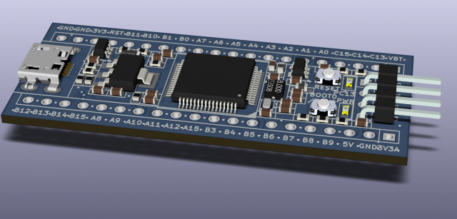
I merged the pull request as soon as I got the notification email
[victor_pv – Wed Dec 20, 2017 11:52 pm] –
Squonk, is this the final one, or are you stil thinking on adding something else?
How about we all first have a good look at it to do a last check for errors/improvements, and then we’ll have some of these produced ![]() .
.
[racemaniac – Thu Dec 21, 2017 1:01 am] –
How about we all first have a good look at it to do a last check for errors/improvements, and then we’ll have some of these produced
I’m inpatient ![]() , but my question was more directed at the whole design, whether it has all components and features he wanted, or he is still working on adding things, not if the PCB design was final.
, but my question was more directed at the whole design, whether it has all components and features he wanted, or he is still working on adding things, not if the PCB design was final.
[RogerClark – Thu Dec 21, 2017 12:51 am] –
Looks amazingI merged the pull request as soon as I got the notification email
Indeed, I saw it accepted before I finished posting here!
- Add teardrops => Check https://github.com/svofski/kicad-teardrops
- Panelization => Check pcb-panelizer ( http://blog.thisisnotrocketscience.nl/p … panelizer/)
- Option: Add an IMU somewhere on the bottom PCB size on an SPI or I2C bus to get a fully working flight controller board! i am thinking of an Invensense MPU6000 hooked to an SPI bus in order to get 8ksps performance
- Option: Add an RGB LED => 0603?
- Option: Add MCP73831 LiPo battery charger (would require an ideal diode like D3/FET2/R6 in the Olimexino ATMega32U4 schematics)
- Add pad/pin for VBUS for external PA9 VBUS_SENSE feature (USB Host) => Added a series resistor between VBUS and PA9 to avoid short-circuits
- Provide footprint for parallel capacitor near SDCard and voltage regulators
- Option: add an SPI Flash chip as an alternative to SDCard connector (overlapping footprints)
- Add optional shunt resistors to route a single bit SPI bus to the SDCard connector for devices without SDIO interface => NOT POSSIBLE, too tight!
The first 2 items are required steps to launch the final PCBs, but not strictly required for prototypes.
Many of the remaining items are options that need to be discussed/prioritized ar’least to see what will be included in the first version.
But as @racemaniac pointed out, there must be a previous check on the current design for possible improvments/errors.
And of course, this is a collaborative design and all input is welcomed!
I found the other day this webpage does an autmated DFM check for free, no need to register or anything:
http://instantdfm.bayareacircuits.com/
Besides checking minimum track separation, pad size, track to pad separation pad to pad, etc, if it doesn’t find anything wrong, at the end shows a set of pictures of the smallest features detected, which may help detect other errors. Just posting it here in case anyone wants to use it.
Unfortunately, PA4-7 is crammed on the pins closest north of the STM32 on the BluePill board, and this is the same situation south of the STM32 for PA15+PB3-5 pins, so these signals are difficult to use for onboard chips such as SPI Flash or IMU. PB9-10+PC2-3 is spread all over the board, so not usable either.
This only leaves the possibility to use SPI1 on PB12-15, because the corresponding pins are located at the bottom left of the board and are close to each other. But the free PCB space in this region is tight, unless the SDCard connector is not mounted. This means that this SPI1 pin configuration may be suitable for an SPI Flash chip as an alternative to mounting the SDCard connector, which sounds reasonable. Of course, this is subject to being able to add the SPI Flash footprint on bottom side, as an alternative footprint to the SDCard connector.
This also rules out the SPI bus interface mentioned before for the IMU. The IMU can however be controlled using I2C with a limited 4ksps rate and located between or beneath the 2 button switches, where there is still some room. This sample rate is not ridiculous, most of the current flight controllers are still limited to 4ksps, only the latest ones switched to SPI and chips that can handle 8 or 16ksps.
What do you think?
Also, adding the IMU for example would be epic, there are tons of other things you can think of (high quality DAC, LIon charger, stepper driver, …) that would be nice to haves, but it’ll never be in the same league as a board build for the purpose this one might then serve.
Also, if we ever have this produced, would they really like it to be able to make multiple boards with the same pcb design (is it really that much of a cost saver), or is there really a market for people who’ll later on solder a qfn motion sensor themselves (not easy to do).
I’d stick with the board as it currently is.
From my previous post, it seems obvious that routing an SPI bus to the built-in SDCard connector is utopia.
However, adding a pad/pin for VBUS for external PA9 VBUS_SENSE (USB Host) may be an interesting feature: we may re-purpose one of the 2 GND pins near the micro USB connector to output VBUS through a 0R shunt, to be mounted only when the USB Host feature is required.
It may also be possible to add parallel decoupling capacitors on the SDCard and the U1 LDO.
As the current micro USB connector is a little bit shorter than the previous Molex part, this leave some (little) room for adding a 0603 footprint close to VBUS, and it seems relatively easy to route the PA9 signal close to it.
The point is that it is now possible to perform this connection onboard instead of externally, like proposed previously: if we add a series 560 ohm resistor between VBUS and PA9 like the micropython board, this prevents short-circuits if PA9 is driven low (i ~= 9 mA, P ~= 44 mW). PA9 is 5V-tolerant, so no voltage divider is required, and if strict compatibility with the original Bluepill is required, one can unsolder this resistor to disconnect the signals, but at least, there is no risk for a blue smoke. And there is no real need to breakout the VBUS signal otherwise.
I think it is also possible to remove the R12 pull-up resistor on SDIO_D3 and replace it with a second parallel 100 nF (unmounted?) capacitor across SDCard voltage supply for better decoupling if required. The reason for the R12 resistor is unclear, I probably just took the micropython board as an example, but in their case it is only used for fixing the voltage level at boot time for securing the ROM bootloader, which seems not to cause particular problems based on our experience.
[Squonk42 – Sat Dec 23, 2017 1:02 pm] –
I looked further at the PA9/VBUS_SENSE to VBUS connection for the USB Host feature.As the current micro USB connector is a little bit shorter than the previous Molex part, this leave some (little) room for adding a 0603 footprint close to VBUS, and it seems relatively easy to route the PA9 signal close to it.
The point is that it is now possible to perform this connection onboard instead of externally, like proposed previously: if we add a series 560 ohm resistor between VBUS and PA9 like the micropython board, this prevents short-circuits if PA9 is driven low (i ~= 9 mA, P ~= 44 mW). PA9 is 5V-tolerant, so no voltage divider is required, and if strict compatibility with the original Bluepill is required, one can unsolder this resistor to disconnect the signals, but at least, there is no risk for a blue smoke. And there is no real need to breakout the VBUS signal otherwise.
I think it is also possible to remove the R12 pull-up resistor on SDIO_D3 and replace it with a second parallel 100 nF (unmounted?) capacitor across SDCard voltage supply for better decoupling if required. The reason for the R12 resistor is unclear, I probably just took the micropython board as an example, but in their case it is only used for fixing the voltage level at boot time for securing the ROM bootloader, which seems not to cause particular problems based on our experience.
hadn’t noticed the pullup on the d3 line yet, indeed, best to remove it.
when using the sd card, just enable the internal pullups of the stm32 on the datalines, and it’ll be fine ![]()
What do you think about the series resistor between VBUS and PA9?
[Squonk42 – Sat Dec 23, 2017 1:24 pm] –
OK, I will do that!What do you think about the series resistor between VBUS and PA9?
i think it’s also ok, but i’m a bit too tired & with my mind elsewhere to think it through XD
- Add teardrops => Check https://github.com/svofski/kicad-teardrops
- Panelization => Check pcb-panelizer ( http://blog.thisisnotrocketscience.nl/p … panelizer/)
- Option: Add an IMU somewhere on the bottom PCB size on an SPI or I2C bus to get a fully working flight controller board! i am thinking of an Invensense MPU6000 hooked to an SPI bus in order to get 8ksps performance I2C bus, as no SPI bus is available easily onboard with the real estate for the chip
- Option: Add an RGB LED => 0603?
- Option: Add MCP73831 LiPo battery charger (would require an ideal diode like D3/FET2/R6 in the Olimexino ATMega32U4 schematics)
- Option: add an SPI Flash chip as an alternative to SDCard connector (overlapping footprints)
And here is a 3D view of the result:
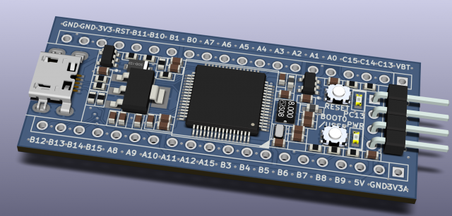

But I would prefer that one from Squonk. I think it is designed with due diligence.
but i’d also prefer what we currently have, nice small format, and sd card on the board itself
The header, USB connector and button switch looks cheap, but the price isn’t: 99 RMB is $15, and that is on Taobao…
I don’t know yet how much our BluePill F4 will cost, but I hope to keep the price between $5 and $10. Of course, this depends on volume and if we find someone to build it in Mainland China or not.
[Squonk42 – Sat Dec 23, 2017 1:02 pm] –
I think it is also possible to remove the R12 pull-up resistor on SDIO_D3 and replace it with a second parallel 100 nF (unmounted?) capacitor across SDCard voltage supply for better decoupling if required. The reason for the R12 resistor is unclear, I probably just took the micropython board as an example, but in their case it is only used for fixing the voltage level at boot time for securing the ROM bootloader, which seems not to cause particular problems based on our experience.
If I remember right, SDIO_D3 also has a function as SDCard detect when no card detect switch exists. I’m trying to find all the information, from what I remember there is a pull up of 1M or so internally in the sdcard, that can be disconnected with a command.
No idea why would need a resistor in series, but may have something to do with it, and likely carried from another board design.
If I can find more information on this, which should be somewhere in the internet, I’ll post it.
There is some mention about that pull up here:
https://www.sdcard.org/cht/downloads/pl … E1_100.pdf
Found a bit more infor, it’s 50K and pull up, page 20:
http://datasheet.octopart.com/IP4052CX2 … 555750.pdf
There are some circuits showing a 570K pull down externally. My guess is that’s used to ensure the line is down while a card is not connected, so card detection can effectively detect when one is connected and the line is pulled up.
Having a external pull-up would negate the card detection feature completely, so I can only guess that R12 is not related to card detection at all, and likely as Squonk thought is used for boot.
Olimex is using the 1M pulldown “sdcard detect” trick since ever.
The trick is about an internal pullup resistor (~200k ~50k) inside the sdcard which pulls the line to Vcc when inserted (otherwise 0 due to 1M).
Thus you read (DAT3 below) 1 when the sdcard is inserted, otherwise you read 0.
- 1M sdcard detect.JPG (37.49 KiB) Viewed 337 times
This rules out R12 pull-up completely. In the micropython schematic, it is clearly part of their scheme to fix the voltage of input pins used by the ROM bootloader.
I am a little bit nervous with pull-up/down values in Mohms: because of their high resistance value, they are very sensitive to ESD, as a small current will be enough to cause a significant voltage glitch. OTOH, if Olimex is using this trick for ages…
[Squonk42 – Sun Dec 24, 2017 4:57 pm] –
I am a little bit nervous with pull-up/down values in Mohms: because of their high resistance value, they are very sensitive to ESD, as a small current will be enough to cause a significant voltage glitch. OTOH, if Olimex is using this trick for ages…
STM had ESD protection in the SDCard pins int heir 3d printer board, with one of their chips for specifically that purpose (ESD protection for SDcard ports). It’s an option, but would add another footprint to route in the PCB and another part to the BOM.
The second link I added shows a 470K pull down, still pretty high, but half of the Megaohm ones ![]()
[Squonk42 – Sun Dec 24, 2017 4:57 pm] –
Thank to both of you for looking at it!This rules out R12 pull-up completely. In the micropython schematic, it is clearly part of their scheme to fix the voltage of input pins used by the ROM bootloader.
I am a little bit nervous with pull-up/down values in Mohms: because of their high resistance value, they are very sensitive to ESD, as a small current will be enough to cause a significant voltage glitch. OTOH, if Olimex is using this trick for ages…
Normally the pins need a pull-up ( if we use those of the stm32 it’s 40k I think). The default pull-up of 200k is probably chosen to not affect the real pullups too much when put in parallel with them. When we put a pulldown for card detection, it’ll make a voltage divider with the 200k pull-up, so anything below 400k will cause the resulting voltage to be too close to VCC/2 (or even below it) when the card is inserted, so it’s logical to choose something big like 1M
No problem with 1M pulldown as it is active only during “card detect read of the DAT3”. When the card is not inserted you have to read 0, thus the parasitic pullup resistances shall be kept high at that line.
The only source of voltage at the 1M when sdcard not inserted, imho, is the reverse current of the high-side clamp diode (pin’s built-in ESD protection) which could be something around 100mV max (Ir=100nA worst case).
Otherwise there could be the stm32’s pullup (say 40k || 200k 50k) active as Victor wrote (that eliminates the 1M “sensitivity”).
PS: many sources say the internal sdcard DAT3 pullup is ~50k. Some specs say it is 10k-90k Min-Max. Some 50k +/- 20%.
There is the ACMD42 command which switches the pullup on/off when required..
PPS: The latest SD Physical Layer Simplified Specification v6.0 (page 11) says “At power up this line has a 50k pull up enabled in the card”.
[victor_pv – Sun Dec 24, 2017 7:06 pm] –[Squonk42 – Sun Dec 24, 2017 4:57 pm] –
I am a little bit nervous with pull-up/down values in Mohms: because of their high resistance value, they are very sensitive to ESD, as a small current will be enough to cause a significant voltage glitch. OTOH, if Olimex is using this trick for ages…STM had ESD protection in the SDCard pins int heir 3d printer board, with one of their chips for specifically that purpose (ESD protection for SDcard ports). It’s an option, but would add another footprint to route in the PCB and another part to the BOM.
The second link I added shows a 470K pull down, still pretty high, but half of the Megaohm ones
ESD protections are mandatory in an end-user product on all connectors, buttons, LEDS, etc. that are accessible externally in order to comply with EMC rules. In this case, TVS protection diodes must be used, such as PRTR5V0U2X for the USB connector, dual PRTR5V0U4D for the SDCard connector, and individual 0603 bidirectional ESD TVS diodes on buttons and LEDs. Products featuring high resistance values are also subject to a more subtle ESD problem, where this resistor is acting as an antenna for ESD surface currents on the enclosure (thus my fear, not counting for additional thermal noise).
But for a prototype board like this, the whole PCB is exposed anyway, so you are supposed to use them in an ESD-safe environment only (you always wear your ESD wrist strap, do you? ![]() ), and there is thus an exemption for this kind of products. This is why there are no ESD protections at all on our BluePill f4 board, this would add to the BOM cost without adding much effective protection anyway.
), and there is thus an exemption for this kind of products. This is why there are no ESD protections at all on our BluePill f4 board, this would add to the BOM cost without adding much effective protection anyway.
Note that this may cause a problem if this board is naively integrated as-is in an end-user product, though…
Please note also that for a bullet-proof EMC USB design, we would need to add a common-mode choke on USB data lines to avoid common-mode noise pollution, ferrite beads on on power USB power supply to filter out high-frequency noise, and high-voltage (500V) capacitor with parallel 1M resistor between shield protective Earth and ground in order to achieve proper GND level alignment upon cable insertion… Not implemented here for the same reason as above!
[Pito – Mon Dec 25, 2017 11:45 am] –
I am a little bit nervous with pull-up/down values in Mohms: because of their high resistance value, they are very sensitive to ESD, as a small current will be enough to cause a significant voltage glitch.
No problem with 1M pulldown as it is active only during “card detect read of the DAT3”. When the card is not inserted you have to read 0, thus the parasitic pullup resistances shall be kept high at that line.
The only source of voltage at the 1M when sdcard not inserted, imho, is the reverse current of the high-side clamp diode (pin’s built-in ESD protection) which could be something around 100mV max (Ir=100nA worst case).
Otherwise there could be the stm32’s pullup (say 40k || 200k 50k) active as Victor wrote (that eliminates the 1M “sensitivity”).PS: many sources say the internal sdcard DAT3 pullup is ~50k. Some specs say it is 10k-90k Min-Max. Some 50k +/- 20%.
There is the ACMD42 command which switches the pullup on/off when required..
PPS: The latest SD Physical Layer Simplified Specification v6.0 (page 11) says “At power up this line has a 50k pull up enabled in the card”.
There is not much room to add a new 0603 footprint near the SDIO_D3 signal. Do you think that this “SDCard Detect” feature is required and if so, should we sacrifice one the 2 decoupling capacitors on the SCard connector to get it on board?
[Squonk42 – Mon Dec 25, 2017 4:08 pm] –[Pito – Mon Dec 25, 2017 11:45 am] –
I am a little bit nervous with pull-up/down values in Mohms: because of their high resistance value, they are very sensitive to ESD, as a small current will be enough to cause a significant voltage glitch.
No problem with 1M pulldown as it is active only during “card detect read of the DAT3”. When the card is not inserted you have to read 0, thus the parasitic pullup resistances shall be kept high at that line.
The only source of voltage at the 1M when sdcard not inserted, imho, is the reverse current of the high-side clamp diode (pin’s built-in ESD protection) which could be something around 100mV max (Ir=100nA worst case).
Otherwise there could be the stm32’s pullup (say 40k || 200k 50k) active as Victor wrote (that eliminates the 1M “sensitivity”).PS: many sources say the internal sdcard DAT3 pullup is ~50k. Some specs say it is 10k-90k Min-Max. Some 50k +/- 20%.
There is the ACMD42 command which switches the pullup on/off when required..
PPS: The latest SD Physical Layer Simplified Specification v6.0 (page 11) says “At power up this line has a 50k pull up enabled in the card”.There is not much room to add a new 0603 footprint near the SDIO_D3 signal. Do you think that this “SDCard Detect” feature is required and if so, should we sacrifice one the 2 decoupling capacitors on the SCard connector to get it on board?
Not having an sd card detect is quite annoying i think :s. so if possible it would be *really* nice to have.
[racemaniac – Mon Dec 25, 2017 9:29 pm] –[Squonk42 – Mon Dec 25, 2017 4:08 pm] –[Pito – Mon Dec 25, 2017 11:45 am] –
No problem with 1M pulldown as it is active only during “card detect read of the DAT3”. When the card is not inserted you have to read 0, thus the parasitic pullup resistances shall be kept high at that line.
The only source of voltage at the 1M when sdcard not inserted, imho, is the reverse current of the high-side clamp diode (pin’s built-in ESD protection) which could be something around 100mV max (Ir=100nA worst case).
Otherwise there could be the stm32’s pullup (say 40k || 200k 50k) active as Victor wrote (that eliminates the 1M “sensitivity”).PS: many sources say the internal sdcard DAT3 pullup is ~50k. Some specs say it is 10k-90k Min-Max. Some 50k +/- 20%.
There is the ACMD42 command which switches the pullup on/off when required..
PPS: The latest SD Physical Layer Simplified Specification v6.0 (page 11) says “At power up this line has a 50k pull up enabled in the card”.There is not much room to add a new 0603 footprint near the SDIO_D3 signal. Do you think that this “SDCard Detect” feature is required and if so, should we sacrifice one the 2 decoupling capacitors on the SCard connector to get it on board?
Not having an sd card detect is quite annoying i think :s. so if possible it would be *really* nice to have.
OK, actually, the main LDO U1 and the SD Card connector are very close to each other, so we can remove one decoupling capacitor safely. I will then add the 1M pull-down resistor on SDIO_D3 to get the SDCard detect feature.
I started to add a 1616 (“0603”) RGB LED to replace the red LED D2: it is possible to get a footprint which is compatible with both, so a cheap version will have only the red one, and as an option (more expensive?), we can get an RGB LED by mounting 2 resistors to connect the blue and green cathodes to PA14 and PA13, respectively. These signals are only used for SWD, so it will add some colors during flashing ![]()
Unfortunately, AFAICT PA13/PA14 and PC13 do not have PWM capabilities.
Btw, the only way how to get an sdcard under full control for ie. a “hot-swapping” or a “recovery” from a crashed sdcard is to have the sdcard’s Vcc power switchable on/off (ie. via a high-side pmosfet, etc.).. And the OS/core must support that option as well..
An another point is an sdcard possesses a ~uF decoupling capacitor inside, so a hot-insertion of the sdcard could cause a current surge resetting the mcu. Thus powering the sdcards requires a careful design (ie. a separate voltage regulator, LC filter, large capacity low ESR capacitor, etc)..
https://forum.arduino.cc/index.php?topi … msg2214450
[Pito – Tue Dec 26, 2017 10:58 am] –
Not having an sd card detect is quite annoying i think :s. so if possible it would be *really* nice to have.
Btw, the only way how to get an sdcard under full control for ie. a “hot-swapping” or a “recovery” from a crashed sdcard is to have the sdcard’s Vcc power switchable on/off (ie. via a high-side pmosfet, etc.).. And the OS/core must support that option as well..An another point is an sdcard possesses a ~uF decoupling capacitor inside, so a hot-insertion of the sdcard could cause a current surge resetting the mcu. Thus powering the sdcards requires a careful design (ie. a separate voltage regulator, LC filter, large capacity low ESR capacitor, etc)..
https://forum.arduino.cc/index.php?topi … msg2214450
Ooh, thanks for the extra info, was wondering about the first (what to do when an sd card crashes, if you could resolve it via software)
it’s odd that you can’t >_<…
And i already ran into the sd card resetting the mcu on my lightsaber boards, but if we put a 4.7uF capacitor across it (as in the current design), isn’t that already enough?
Well, we can’t afford to have a PM for the SDCard only, unfortunately.
As for the inrush current, the AP2114 looks like it has a 40mV dip @1A using the same 4.7µF caps that we use here, so I hope it will be good enough not to reset the STM32. We may have to test and adjust the capacitor values/types.
- Add teardrops => Check https://github.com/svofski/kicad-teardrops
- Panelization => Check pcb-panelizer ( http://blog.thisisnotrocketscience.nl/p … panelizer/)
- Option: Add an IMU somewhere on the bottom PCB size on an SPI or I2C bus to get a fully working flight controller board! i am thinking of an Invensense MPU6000 hooked to an SPI bus in order to get 8ksps performance I2C bus, as no SPI bus is available easily onboard with the real estate for the chip
- Option: Add MCP73831 LiPo battery charger (would require an ideal diode like D3/FET2/R6 in the Olimexino ATMega32U4 schematics)
- Option: add an SPI Flash/FRAM chip as an alternative to SDCard connector (overlapping footprints)
And here is a 3D view of the result:
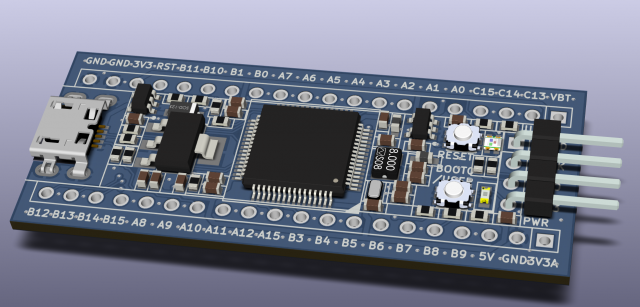
[racemaniac – Wed Dec 27, 2017 7:23 am] –
btw, maybe time to do an update of the BOM?
I created a pull request with updated BOM (BOM files were in .gitignore ![]() ). I added the PDF files for schematic and layout at the same time.
). I added the PDF files for schematic and layout at the same time.
The problem is the internal sdcard capacitor is a multilayer ceramic one with ultra low ESR.
When you connect such an empty capacitor to the voltage regulator, the inrush current is limited by its parasitic serial resistance only (as well as by its serial inductance which is rather small ~xx nH) – that Rs could be say 0.005ohm (add contacts and copper resistances). Imagine that current peak (Ipeak = 3.3V/0.0xxOhm) which occurs when the mcu is already running (upon powering on your lightsaber the peak is there as well, but the mcu is in the “reset state” at that time, thus all is ok).
The 4.7uF capacitor (or better a 10-20uF, must be a ceramic multilayer one) placed close to sdcard’s Vcc may help, sure.
Mind the capacity of a ceramic multilayer capacitor drops significantly with the applied bias voltage (up to -80% at max allowed voltage), better use a capacitor for 15-25V, and X7R type.
A series inductor (a few hundred nH) helps to limit the rising edge of the inrush current too..
The Olimex design reflects that issue it seems:
viewtopic.php?f=19&t=2633&start=530#p39114
I think I can fit the same inductor as Olimex (LQW2BASR47J00L) which is a relatively large 0805 footprint, but I cannot add more capacitors than the 4.7µF 6.3V X7R 0603 already installed. We can replace it with a 10µF with same other characteristics if required. Do you think we should be OK with this setup?
The best way is to do an experiment and to measure the transient upon insertion..
Are there any Olimex F407 boards users? They may provide a measurement (put oscilloscope probe (1:10) at the sdcard’s Vdd socket pad, power on the board, wait say 5secs, insert a card, watch the Vdd transient).
We have the AP2114HA-3.3TRG1 LDO D1 nearby with its 2 output capacitors C8 (4.7µF 6.3V X7R 0603) and C18 (100nF 50V X7R 0603), then the inductor above in series with the SDIO_VDD, then C&6 (another 4.7µF 6.3V X7R 0603), all in a tight space. We can change the values or put a ferrite bead and experiment, I guess.
Many of the SDIO Card interface I have seen on dev boards (some much larger than our BluePill) do not provide such a luxurious filtering, probably because they don’t consider hot swapping the card.
On a layout point of view, there won’t be much more I will be able to stuff in there, so I will release a new version with the additional 0805 footprint in series with the SDCard power supply, we will have to test.
Unfortunately, I don’t have an Olimex F407 board available to test for the Vdd transient ![]()
I would not go with that one..
I would rather go with 150-330nH but w/ lower R and higher I (and lower Q).
The another option is a “ferrite bead” – they are rated in ohms, like 22..1000ohm (an wideband impedance) but for >=1A currents (Rs=0.0xxohm).
For example:
https://eu.mouser.com/Passive-Component … _/N-bw7pa/
https://eu.mouser.com/productdetail/mur … 5UCw%3D%3D
http://www.mouser.com/ds/2/281/c51e-794816.pdf
They are easily to get in 0603 as well.
Anyhow, the best way to design that luxurious filtering is to measure how it works in situ.. ![]()
PS: if it fits leave the 0805 pads there and you may experiment with the best type of inductor/FB.
Worst case you may deploy a 0ohm resistor there when the luxurious LC would not be required.
- SDCArd Inductor.png (56.31 KiB) Viewed 234 times
1) on the bottom layer, under the cpu, one of the sd card traces makes a stupid little zigzag & corner ^^’. easy to fix
2) kicad seems to have some issues with some traces… the drc indeed passes, but on the bottom it still lists 2 traces being unconnected. I thought it simply was an old trace somewhere triggering it (as when having the drc list unconnected things it shows nothing), but when doing a clean up tracks & traces, it removes the pb9 trace and the count goes to 3 unconnected items O_o
there’s still something a bit strange about the project.
1) If what you are talking about are the traces circled in red, this is normal: it is part of my attempts to add teardrops to the board. If the trace goes straight, the teardrop will trigger a DRC violation because it is to close to the nearby trace.
As for the one circled in green, I will drag the trace, no problem!
- Teardrops.png (71.12 KiB) Viewed 191 times
2) is something strange indeed. It gave me 2 unconnected in the status text on the bottom left of the pcbnew screen, not sure if it’s also indicated there on ubuntu. but indeed, drc passed
There are also some problems of coordinate comparisons that are done strictly without systematically applying a tolerance value: these ghosts unconnected value are symptomatic ![]()
Let me know if it fixes the problems for you: for me, I no longer get unconnected signals after applying a “Cleanup Tracks and Vias”, nor do I have unconnected signals in the status bar.
I always inspect all the layers I send to the manufacturer with the Gerbview..
I also cleaned up the unnecessary labels in the schematic, and improved the 3D model for the FC-12M crystal.
Let me know if you still experience “Unconnected” wires.
[Squonk42 – Mon Jan 01, 2018 8:40 pm] –
I pushed a new version after checking the generated gerber files with gerbview.I also cleaned up the unnecessary labels in the schematic, and improved the 3D model for the FC-12M crystal.
Let me know if you still experience “Unconnected” wires.
looks better indeed, nothing indicated as unconnected anymore, and a cleanup of tracks & traces doesn’t remove required traces anymore ![]()
Thanks for testing!
I strongly recommend to use FreecAD version 0.17 or later.
– the gnd of ap2112k should be connected to agnd, not gnd
– your alternative to the seperate voltage regulator doesn’t match what you described in your post:
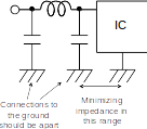
the grounds of the resistors before & after the ferrite bead should have some distance, the resistor after the cap’s ground & the ground of the IC should be as close as possible
this might affect the performance of your alternative to the seperate regulator
I agree on the first remark. On the second one, “apart” is a relative concept, especially on this tiny board ![]()
I am thinking or removing the “CLC” solution to keep only the AP212 (with AGND). What do you think?
On another subject, I think it is very feasible to add an optional LiPo charger circuit based on the Microchip MCP73812 and an “ideal diode” like used in the OLIMEXINO-32U4 :
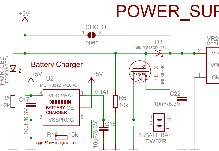
- OLIMEXINO-32U4 LiPo Charger.png (110.36 KiB) Viewed 192 times
[Squonk42 – Sat Jan 06, 2018 9:36 am] –
No problem, the more pairs of eyes, the better!I agree on the first remark. On the second one, “apart” is a relative concept, especially on this tiny board
I am thinking or removing the “CLC” solution to keep only the AP212 (with AGND). What do you think?
On another subject, I think it is very feasible to add an optional LiPo charger circuit based on the Microchip MCP73812 and an “ideal diode” like used in the OLIMEXINO-32U4 :
OLIMEXINO-32U4 LiPo Charger.png
It should fit on the bottom of the board, between the right edge and the SWD connector. I still don’t know where I will connect the battery though…
for me only the second regulator is fine. it’ll probably be more reliable than the other option since it’s indeed hard to properly seperate those grounds.
the charger sounds fun, but that ideal diode is probably not a cheap/easy part to get?
and one thing that’s also bothering me a bit when seeing the 3d model: some of the pads on the bottom are underneath the sd card when it’s inserted? not such a huge problem, also since they’re probably pretty hard to move ^^’
[racemaniac – Sat Jan 06, 2018 9:44 am] – for me only the second regulator is fine. it’ll probably be more reliable than the other option since it’s indeed hard to properly seperate those grounds.
What worries me is that in almost all STM32F schematics that I can find, the +3.3VA is only obtained by filtering the +3.3V using a ferrite bead and a couple of 10µF/6/3V + 100nF capacitors. I just feel that using both a separate LDO and an inductor between AGND and GND is a little bit over-engineered.
[racemaniac – Sat Jan 06, 2018 9:44 am] – the charger sounds fun, but that ideal diode is probably not a cheap/easy part to get?
The “ideal diode” here is just the IRLML6402 PMOS and the 1N5819 Schottky diode, along with the 10K resistor to polarize the MOSFET correctly. The IRLML6402 is a very common part, available at all global web distributors, but also on AliExpress and Taobao at a very low price. The 1N5819 Schottky diode is the same that we are already using for the connection between VUSB and +5V, so cheap too.
All components are easy to solder by hand (no QFN…), so they could be added by a motived DYI person afterwards, or sold as an option.
For the battery connection, I think I will only provide a simple 1mm drill TH for VBAT (and rename the existing pin VBAT to VBK to avoid confusion, as it is more for RTC backup), the question is where to put this pad: it is huge ![]()
[racemaniac – Sat Jan 06, 2018 9:44 am] – and one thing that’s also bothering me a bit when seeing the 3d model: some of the pads on the bottom are underneath the sd card when it’s inserted? not such a huge problem, also since they’re probably pretty hard to move ^^’
Yes, these are the pads for PC6/PC7. But these signals are quite important, as they are the only way to get the I2S2_MCK/I2S3_MCK signals.
I will see what I can do: it looks like I can route PC7 under the PC6/SDIO_D2/SDIO_D3 traces, then use a via to cross the SDIO bus and have the PC7 pad close to the other ones. For PC6, I can probably move up the PB15/PB14 pads to route a trace on top between SDO_D0 and PB15, then have the PC6 pad close to the other ones.
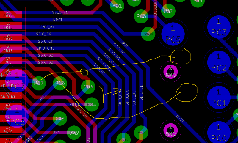
- BluePillF4 PC6-7.png (154.8 KiB) Viewed 194 times
a) You do not need battery connected when doing programming via SWD..
b) You may not need Vcc connected on the Vcc pin while programming..
[Pito – Sat Jan 06, 2018 2:14 pm] –
Can you reuse the Vcc/Gnd pins from the SWD header for the battery as well

a) You do not need battery connected when doing programming via SWD..
b) You may not need Vcc connected on the Vcc pin while programming..
Yes! So, I added a 0R between the SWD +3.3V pin (now +VBAT) and the +3.3V signal, so:
- it behaves like on the BluePill if there is no LiPo charger circuit, the +3.3V pin on the SWD header is an input that will compete with the LDO output (bad
 )
) - if you have a LiPo charger circuit and no battery connected, just connect the SWD +3.3V power to the +3.3V pin on the header near the NRST pin (still bad )
- better: feed the board from +5V or USB if no battery or no battery charger circuit!
- but if you have a LiPo charger circuit and a battery connected, just don’t connect the pin to anything and use the battery power
On other subjects, I fixed the AGND problem on the analog LDO and separated the GND pads on the capacitors in the CLC filter option: actually, one is now on AGND, the other on GND and much farther apart.
I also have the Olimex LiPo charger circuit routed, I just need to clean up all this mess before committing the changes.
[Squonk42 – Tue Jan 09, 2018 10:04 pm] –[Pito – Sat Jan 06, 2018 2:14 pm] –
a) You do not need battery connected when doing programming via SWD..
b) You may not need Vcc connected on the Vcc pin while programming..Yes! So, I added a 0R between the SWD +3.3V pin (now +VBAT) and the +3.3V signal, so:
- it behaves like on the BluePill if there is no LiPo charger circuit, the +3.3V pin on the SWD header is an input that will compete with the LDO output (bad
- if you have a LiPo charger circuit and no battery connected, just connect the SWD +3.3V power to the +3.3V pin on the header near the NRST pin (still bad
- better: feed the board from +5V or USB if no battery or no battery charger circuit!
- but if you have a LiPo charger circuit and a battery connected, just don’t connect the pin to anything and use the battery power
On other subjects, I fixed the AGND problem on the analog LDO and separated the GND pads on the capacitors in the CLC filter option: actually, one is now on AGND, the other on GND and much farther apart.
I also have the Olimex LiPo charger circuit routed, I just need to clean up all this mess before committing the changes.
sounds great ![]()
[Pito – Wed Jan 10, 2018 9:57 am] –
Actually, routing is not that bad, there is still some unused space left ![]()
The idea is to get an F4 version of the BluePill board, if possible made by a Chinese manufacturing house. IMO, a large part of the success of the BluePill board is because of its cheap price: it’s in the same ball park as the Arduino Pro Mini @$1.72. You can get cheaper boards featuring ATMega 168, ATTiny85 or down to STM8S103F3P6 @$0.66, but you get so much more power with the BluePill…
OTOH, you can get much more powerful chips with a little more money, including ESP8266 and ESP32.
So if there is a sweet spot for an F4 BluePill, it must be at the lowest possible cost, with the benefit of raw CPU power and numerous peripherals with DMA.
Most people here are very concerned about price, so I think we should stick to a 2-layer design only. I admit 4 layers would bring better performance (including for EMC reasons), but then, you can always add the GND and power layers and clean up traces if required for your needs.
Let’s try to get some prototypes working, then if we need to change things for another revision because there is too much noise or whatever else, can be done later.
- Main thing: I added a LiPo battery charger as an option on the bottom of the board below the SWD connector. It uses the same MCP73812T-420I/OT and ideal diode made up of a PMOS FET transistor and a Schottky diode as Olimex in its OLIMEXINO-32U4 board. The battery has to be connected to the 2 extreme pins on the SWD header,
as there are other ways to power the board anyway. If the charger option is not installed, a 0R mounted on the board top side makes it strictly compatible with the original Bluepill by connecting it to +3V3 - The GND on the analog LDO is now on AGND
- The alternative (simpler) analog power supply using a CLC filter is now laid out better
- The VBUS_EN pin has been changed from PC4 to PC0, as this pin is less useful for anything else
- The pads on the bottom side of the board for PC1-PC7 are now aligned and no longer below the SDCard, with a nice 1.27 mm pitch
Here is what it looks like:
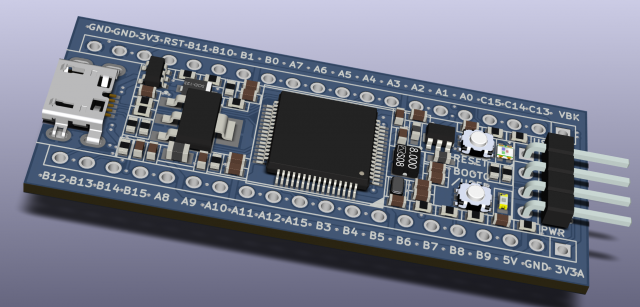
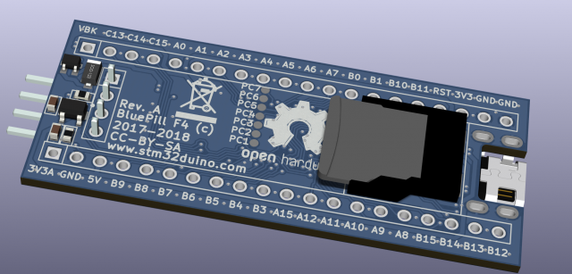
Please let me know if you find a problem, or just if you want to discuss regarding the board!
[Squonk42 – Sat Jan 13, 2018 9:01 pm] –
I pushed a new version of the BluePill F4 board with the following features:
- Main thing: I added a LiPo battery charger as an option on the bottom of the board below the SWD connector. It uses the same MCP73812T-420I/OT and ideal diode made up of a PMOS FET transistor and a Schottky diode as Olimex in its OLIMEXINO-32U4 board. The battery has to be connected to the 2 extreme pins on the SWD header,
as there are other ways to power the board anyway. If the charger option is not installed, a 0R mounted on the board top side makes it strictly compatible with the original Bluepill by connecting it to +3V3- The GND on the analog LDO is now on AGND
- The alternative (simpler) analog power supply using a CLC filter is now laid out better
- The VBUS_EN pin has been changed from PC4 to PC0, as this pin is less useful for anything else
- The pads on the bottom side of the board for PC1-PC7 are now aligned and no longer below the SDCard, with a nice 1.27 mm pitch
Here is what it looks like:
Please let me know if you find a problem, or just if you want to discuss regarding the board!
niiiice XD
one tiny remark though: there’s a silk screen line going trough the pc7 pad ![]() (although when plotting the gerbers, you can substract it from the silk screen
(although when plotting the gerbers, you can substract it from the silk screen ![]() ).
).
Yea, imagine this board is pressed into a solderless-breadboard (for example), and usually with a significant force.. Messing with the sdcard would be a pain..
when making my own boards i’m always doubting between both options. Having it easily reachable during development is nice. When building it into something it however is nice to have the sd card nicely protected on the belly of the board
Like Maple Mini did..
You must not see the chip, and you will get more place for silk screen messages and logos
PS: the PC1-PC7 will become better accessible too. The Q is the usb socket – it could stay as-is, if you ask me.. ![]()
[racemaniac – Sun Jan 14, 2018 8:43 am] – niiiice XD
one tiny remark though: there’s a silk screen line going trough the pc7 pad
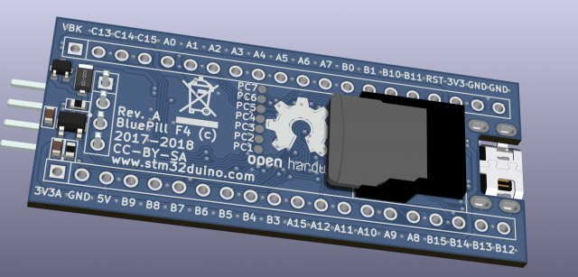
[Pito – Sun Jan 14, 2018 11:54 am] –
Another option is to have the current bottom the new top.. Sdcard will stay as-is, but leds and buttons have to be placed on the new top.. That could be easy as there is nothing beneath the leds and buttons currently..
Like Maple Mini did..
You must not see the chip, and you will get more place for silk screen messages and logosPS: the PC1-PC7 will become better accessible too. The Q is the usb socket – it could stay as-is, if you ask me..
that would then break the point of the basic items of the board (the bluepill compatible part) all being on 1 side
PS: you have to add the SWD header pins description on the bottom then..
[ChrisMicro – Sun Jan 14, 2018 9:24 am] –
Your design looks very nice. Probably it would be useful if the SD-Card Holder would be turned by 180°. It could be easier for a user to exchange the SD-card when the board is built in a housing.
At one point in time, I had the SDCard turned 180°, but I figured out it would not be easy to access it anyway, since the micro-USB plug probably be in the way. And this is no fancy push-push SDCard holder…
But I may be wrong. If this is the case, there is a nice puzzle to solve when reordering the traces below the STM32 ![]()
EDIT: below you can see what I mean (I just put the SDCard holder on an original BluePill):
With this MCU, the micro USB connector, a (larger but beefier) LDO, 2x (smaller) crystals, 2x buttons (vs. 1x, lower profile), 2x LEDs, the SWD header, 1 additional Schottky diode, 13 resistors (vs. 8), 15 capacitors (vs. 13), 2 inductors (vs. none) and no cumbersome jumper block, this should be in the same $2~$3 ballpark as the original BluePill, but with more buttons for reset, boot selection and custom application usage, a correct USB pull-up resistor, a VUSB/+5V reverse current diode protection and more power… All with a lower profile (flat bottom), as the tallest part besides the SWD header are the LDO and the micro USB connector (< 2 mm). EDIT: and better analog supply too!
Here is the new “BluePill F1”:
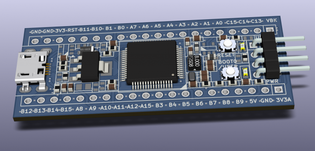
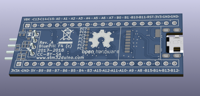
As traces and pads on a PCB cost nothing except for the time you spend laying them out, it may be a good opportunity to etch some useful circuit that may be commonly used by developers. This is why I started by adding the LiPo charger circuit above as a nice option ![]()
I checked existing STM32 designs for more ideas: ST own Nucleo and Discovery boards, 3rd-party boards like Olimex or Itead, language-oriented Espruino and pyboard boards, and also some more specific boards for flight controllers or autopilots like Pixracer and Paparazzi.
In no particular order, here is a list of possible integration candidate circuits:
- Audio (I2S codec or analog interface to ADC/DAC): probably too big to fit and not of general interest
- 2.4GHz RF module: too big
- LCD/OLED screen: like the NodeMCU+OLED combo
- Micro-joystick (on bottom face?)
- Reset controller chip
- Ethernet: too big
- USB TVS: would be difficult to add as an option, and not required on a bare dev board unless it is integrated into a product
- RS232 buffer
- Bluetooth module: too big
- Coin-cell battery or “Gold Cap” for RTC
- FRAM/Flash SPI chip (SOIC8): tried to fit a footprint as an alternative to the SD Card connector, but this results in turning the nice (small) GND plane below the main LDO to pieces => not good
- MOSFET for power output (buzzer, relay, etc.): how to make it optional?
- Battery voltage resistor divider
- CAN transceiver
- 3, 6 or 9-axis IMU (Inertial Measurement Unit), e.g. accelerometer, gyroscope, magnetometer, pressure sensor (altitude): problem is most of them are soldering iron-unfriendly QFN packages These are used of course in all flight controller or autopilot boards, but also on more general-purpose boards like the ST boards (they sell MEMs…) and pyboard, for example…
- “FrSky Inverter”, e.g. a dual XOR gate to invert the level of UART signals as used by this common R/C protocol
- …
Please let me know what do you think of this, or if you have even more circuits to propose!
May be a good option if routing one of the i2c ports there is easy, since it’s just 2 data lines and power.
Not sure how frequently other people use them, I have used them a couple of times to avoid wearing out the flash, but the board already has sdcard for stg too…
I2C FRAM/Flash are 4x to 50x slower than their SPI counterparts, but they may still be useful, you are right. They will then be easier to place in the large empty area below the buttons, and I2C is indeed requiring only 2 signal wires which are easy to find. Maybe a combination of alternative I2C footprints could be nice to have? Like the FRAM/Flash, some I2C sensors, 0.91″ OLED screen, etc?
i think we’re now at a point where it is interesting to order a few boards and build a few prototypes? ![]()
 very nice!
This means that we have around 2 weeks to finish the design, or we will only get the boards on mid-March.
I have most of the components available to make a few boards.
If nobody spots more problems in the current version, then the only thing left is to duplicate the PCB to add the teardrops, at least for a better drill to pad tolerance, mechanical and thermal stress. It looks like the board dimensions are too small for www.allpcb.com to do V-cuts, but they accept tab routing and they propose to do it themselves for free, resulting in a total cost including 24h lead time and TNT shipping to France (3-5 days) for 40 pieces @ $20 (60 pieces are only @ $23 !?!). Unfortunately at this price, the boards will be green, not blue, this adds $8 more ![]()
We do not take many risks by adding footprints on the bottom side for some I2C or other simple devices like voltage divider, MOSFET, etc. But we have to decide what we want asap, as everything will not fit.
Having microSD card is already a killer feature!
As for extra circuit I vote for 1) Extra (F)RAM 2) CAN transceiver 3) Battery resistor driver
– when is it estimated to be available?
– what is the estimated total price for US customers?
Cheers, Ollie
To exchange the SD-card on the bottom side when the F4BP is soldered is probably impossible.
Therefore one solution would be to place the SC-card connector on top btw to flip the whole board as it is before soldering onto a PCB. But then the buttons and leds are also on the bottom and can not be accessed.
So a solution would be to place the SD-card, buttons and leds on top and the rest of the components on bottom.
So, why should someone want to exchange the SD-card?
There are many reasons:
1. The F4 is capable to play MP3 files
2. Someone makes a data logger and wants to transfer the collected 16GB of data by exchanging the SD-card
3. SD-cards are not famous for the life span
[ChrisMicro – Tue Jan 16, 2018 7:26 pm] –
Just one remark to the “SD-card exchange problem”:
To exchange the SD-card on the bottom side when the F4BP is soldered is probably impossible.
<…>
On the surface, your argument is sound. The reality is that I have been playing around with the rPi_Zero-W since they were first available, and it is very, very rare to have to remove the SD card.
Cards today are all wear-leveled and are very tough. A little bit of S/W to manage the filesystem should go a long way to dealing with not needing to remove the card… that is, if using for logging, have an option that spools the file to the serial port of the PC (or USB) and a dialog requesting “Delete?” at the end of the spooling will do necessary housecleaning.
If the board is mounted upside down, small holes in the hosting board or enclosure can be utilized for the buttons. Slap a label over the holes if you want it dust free.
Just thinking out loud.
Ray
Here is how Paul Stoffregen made it with the teensy 3.6.
Just the SD Card connector on the Teensy is $1.90, our connector is $0.30, although not a fancy push/push type.
Anyway, it is not possible to move the SD Card connector on the other side of our board while keeping the original Bluepill pinout compatibility as we have the SWD header on this side.
We are left to leaving the SD Card in its position, either 1) with the same orientation and card removed “under the belly” which is not possible when mounted on a breadboard, 2) turned 180° but then you have to disconnect the USB plug in order to remove the card, 3) flip the whole board upside down with “above the belly” orientation, but then we need to put the buttons and LEDs on the opposite PCB side, and the micro USB connector will be reversed.
I spent 2 hours to turn the SD Card connector 180°, and I have 2 unrouted wires left (SDIO_D3 pull-down and PB12 signal), so solution 2) may be possible, although not easy…
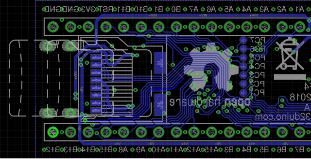
I’m also interested in grabbing some of these – if they come built ![]()
That said, if that’s not possible, I don’t think it’s a major issue to go ahead with our first rev with the card in the original position.
There have been a few people besides Roger that registered to allpcb with the link I posted, so even thought the cost with allpcb went significantly up, we still can get a good bunch of free boards with the credit.
[racemaniac – Wed Jan 17, 2018 9:03 am] –
same here, sd card position is ok for me
+1 or +3
stephen
[Squonk42 – Tue Jan 16, 2018 1:00 pm] –
It looks like the board dimensions are too small for www.allpcb.com to do V-cuts, but they accept tab routing and they propose to do it themselves for free, resulting in a total cost including 24h lead time and TNT shipping to France (3-5 days) for 40 pieces @ $20 (60 pieces are only @ $23 !?!). Unfortunately at this price, the boards will be green, not blue, this adds $8 more
When I do a quote on their system, if I select v-routing for 60 pieces, panel by ALLPCB (so we provide gerbers for a single board and they panelize it), get a quote of $26.
I am setting the dimensions to 16×64 similar to the blue pill.
EDIT: If I just select 60 individual boards, no panel, comes up as $19. Since these are not for industrial production, I would think having the individual boards from the start is just the same as much effort to assemble and reflow as DIY as having them panelized, or anyone sees an advantage on having the panel?
Also, any change to the components in this post?
viewtopic.php?f=19&t=2633&start=360#p37849
Perhaps we should edit Roger’s first post to add the links.
They do not provide Vcut within a panel when the individual board is less than 80x80mm.. (do select “Panel Separating Way:”)
So the only option is, for example, to buy Single PCB, 60pcs 64x16mm, $19 as of today.
PS: It seems they are steadily increasing the prices, 100×100 5pcs $23 today..
@Squonk42: the big blue traces loop in the middle.. would it work?
[Pito – Wed Jan 17, 2018 5:23 pm] –
or anyone sees an advantage on having the panel?
They do not provide Vcut within a panel when the individual board is less than 80x80mm.. (do select “Panel Separating Way:”)
So the only option is, for example, to buy Single PCB, 60pcs 64x16mm, $19 as of today.
PS: It seems they are steadily increasing the prices, 100×100 5pcs $23 today..@Squonk42: the big blue traces loop in the middle.. would it work?
You are right about the price increase for 100×100.
About the v-cut, I have no problem selecting it when I select a board that’s 16×64 and set the panel as 6×2, so 6 boards wide (96mm) and 2 high (128mm).
You can’t have vcuts if the whole panel is smaller than 80×80, but the individual boards being smaller is fine as long as the whole panel is larger.
Comparing in PCB shopper for 100×100 5 or 10 pieces EasyEDA is cheaper while also shipping with DHL.
Anyway we have some free credit for AllPCB, still nothing can’t beat free ![]()
[Pito – Wed Jan 17, 2018 5:23 pm] –
or anyone sees an advantage on having the panel?
They do not provide Vcut within a panel when the individual board is less than 80x80mm.. (do select “Panel Separating Way:”)
So the only option is, for example, to buy Single PCB, 60pcs 64x16mm, $19 as of today.
PS: It seems they are steadily increasing the prices, 100×100 5pcs $23 today..@Squonk42: the big blue traces loop in the middle.. would it work?
Funny, if you enter Qty 60 from radio buttons, you get $19, but when you enter it in the text field and submit, you get $20 ![]()
Where did you get the 64x16mm dimensions from? The actual PCB size is 53.34 mm x 22.86 mm.
OK, here is the selection:

- allpcb_order_form.png (206.82 KiB) Viewed 262 times
[Pito – Wed Jan 17, 2018 5:23 pm] –
@Squonk42: the big blue traces loop in the middle.. would it work?
What do you mean, the SDIO bus? Here are the stats:
Signal	f max. [MHz]	l [mm]	A [mm2]	R [mOhm] w min [mm]    max [mm]	Imax [A]
SDIO_CK	   9094.55	 32.965	0.005	 107.53	 0.152		 0.152	  0.50

SDIO_CMD  10779.22	 27.813	0.005	  90.73	 0.152		 0.152	  0.50

SDIO_D0	   9586.47	 31.273	0.005	 102.02	 0.152		 0.152	  0.50

SDIO_D1	   9740.01	 30.780	0.005	 100.41	 0.152		 0.152	  0.50

SDIO_D2	   9557.50	 31.368	0.005	 102.33	 0.152		 0.152	  0.50

SDIO_D3	   9661.07	 31.032	0.005	 101.23	 0.152		 0.152	  0.50
[victor_pv – Wed Jan 17, 2018 4:10 pm] –
Also, any change to the components in this post?
viewtopic.php?f=19&t=2633&start=360#p37849
Perhaps we should edit Roger’s first post to add the links.
Here is an updated BOM with links to Aliexpress vendors. I suppose everybody has headers from a spare BluePill, but there are a few missing parts (ferrite beads and the battery charger IC, although you can probably get this last one from Microchip as a sample):
- BluePillF4.csv
- (7.89 KiB) Downloaded 150 times
Anyhow, I have to stop with seeing the
[Squonk42 – Wed Jan 17, 2018 8:55 pm] –
Funny, if you enter Qty 60 from radio buttons, you get $19, but when you enter it in the text field and submit, you get $20Where did you get the 64x16mm dimensions from? The actual PCB size is 53.34 mm x 22.86 mm.
OK, here is the selection:
allpcb_order_form.pngI think it could be nice to have BluePill boards that are actually… Blue! But this adds $8 to the bill.
You need to take your eyes of the tracks for a while and relax them, the radio button is for 50 not 60 ![]()
About the size, I thought I saw it in some diagram for the bluepill, but was a while ago and I didn’t pay too much attention to it being right, was just an approximation to see about prices for individual vs panels.
About being blue, is a good point, $8 is not that much more, but being still a prototype, does it matter much? we could order 120 green boards for $29, if anyone is willing to assemble that many…
EDIT: About flipping the sdcard connector, what if instead of flipping it around, you use one that has the pads at the other side instead of underneath? that will flip the sdcard to pull from the other side while keeping the connector pads in the same order.
Like these:
https://www.aliexpress.com/item/10pcs-9 … autifyAB=1
[Pito – Wed Jan 17, 2018 10:03 pm] –
Yea, that fmax is for a straight wire of length l, I think. Such big loop of wires is like a planar transformer
Anyhow, I have to stop with seeing thein the details ..
SDIO is ~25 MHz max, and the lengths are short… There is no better way to fan out these signals unless the Sd Card connector is placed facing south.
Anyway, will will be bitten by a detail that we have not seen, I can bet!
[victor_pv – Wed Jan 17, 2018 10:51 pm] –
You need to take your eyes of the tracks for a while and relax them, the radio button is for 50 not 60
Oups, it was late and I am getting old ![]()
[victor_pv – Wed Jan 17, 2018 10:51 pm] –
About being blue, is a good point, $8 is not that much more, but being still a prototype, does it matter much? we could order 120 green boards for $29, if anyone is willing to assemble that many…
Well, let’s decide, but I don’t think we need that many.
[victor_pv – Wed Jan 17, 2018 10:51 pm] –
EDIT: About flipping the sdcard connector, what if instead of flipping it around, you use one that has the pads at the other side instead of underneath? that will flip the sdcard to pull from the other side while keeping the connector pads in the same order.
Like these:
https://www.aliexpress.com/item/10pcs-9 … autifyAB=1
No, this one is twice the price, and it is too wide to fit between the 2 rows of pins, this is why I selected the current one in the first place. Actually, almost all connectors featuring a push-push mechanism have the same problem.
EDiT: the only one I found was this one from Molex which is 11.95 mm wide, but it is impossible to find on Aliexpress:
http://www.molex.com/molex/products/dat … SOCKET.xml
EDIT2: I actually found them at 1 single vendor, but expensive:
https://www.aliexpress.com/item/10pcs-5 … 95526.html
However, these ones are quite common and cheap:
https://www.aliexpress.com/item/10-PCS- … 38620.html
If squonk sends me a few, that’ll probably cost nearly as much as me just ordering some for myself
I’m wondering if we can’t convince one of the pcb manufacturers to produce 100 of them, and send them in batches of 10 to 10 different addresses for a good price, that would be awesome XD
Racemaniac, I think the shipping from China to multiple places would probably increase the cost. Where are you located?
First class mail in the US is fairly cheap, so I can put a bunch of cards in an envelope for anyone else in the US for just a couple of dollars and should arrive in a few days.
I was thinking on the following:
-Order a batch for Squonk.
-If those are good, order a batch for US, and another for Australia if Roger or someone else is willing to assemble a few over there.
EDIT: Another connector that seems to be short and narrow:
https://www.aliexpress.com/item/20PCS-S … autifyAB=1
I’m trying to find the manufacturer.
Found these diagrams:
https://sc01.alicdn.com/kf/HTB1CbH1JVXX … nector.jpg
https://www.alibaba.com/product-detail/ … 1460XUg6aV
For the one you posted, I found this link that shows a part number and brand seems to be proconn, but can’t find it in google.
https://www.aliexpress.com/item/Mini-TF … autifyAB=1
I just checked sending from belgium to france for example. The very least it’ll cost is 7€ (that is if the total weight is below 350g and it’s not thicker than 5mm)
if it’s more than 350g, it becomes 14€…
at those prices it can quickly become cheaper to just have multiple shipments from china >_<
[victor_pv – Thu Jan 18, 2018 4:34 pm] – EDIT: Another connector that seems to be short and narrow:
https://www.aliexpress.com/item/20PCS-S … autifyAB=1I’m trying to find the manufacturer.
Found these diagrams:
https://sc01.alicdn.com/kf/HTB1CbH1JVXX … nector.jpg
https://www.alibaba.com/product-detail/ … 1460XUg6aV
Unfortunately, this connector is for a full SD Card, not a micro SD one: the width in the diagram is ~27mm:
[victor_pv – Thu Jan 18, 2018 4:34 pm] – EDIT: Another connector that seems to be short and narrow:
For the one you posted, I found this link that shows a part number and brand seems to be proconn, but can’t find it in google.
https://www.aliexpress.com/item/Mini-TF … autifyAB=1
The original part for this one is probably one of these Molex connectors:
http://www.molex.com/molex/products/lis … ductseries
Here are some pictures of the current microSD Card connector on the prototype board, without and with card inserted, then the other “Molex 47309 Series” connector on a LitcheePi board, again without and with card, and a comparison between the current connector and a standard MicrosD connector on the PocketBeagle board:
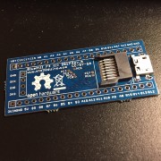
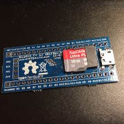
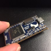
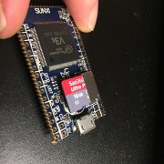
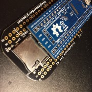
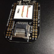
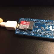
[racemaniac – Thu Jan 18, 2018 4:55 pm] –
i’m from europe (belgium). Not sure how much it would cost for squonk to send some to me (he’s from france, neighbouring country).
I just checked sending from belgium to france for example. The very least it’ll cost is 7€ (that is if the total weight is below 350g and it’s not thicker than 5mm)
if it’s more than 350g, it becomes 14€…at those prices it can quickly become cheaper to just have multiple shipments from china >_<
We are lucky, PCB and parts do not weight much… I check on my kitchen scale, an original Bluepill without header weights only 5g!
And for letters < 3 cm and < 20 g for Belgium, it only costs €1.20 with 3-4 days delivery, and €1.30 for most countries outside Europe. Add a plastic bubble envelope @ €0.20, grand total is €1.50 ($1.85).
I have almost all parts from AliExpress, and enough of them to build ~ 10 boards, except for the STM32 itself, you get the BOM details in my previous post above.
For those ready to do 0603 soldering, I can probably organize the shipping of unmounted PCB+parts to them for performing the initial tests (DON’T EVEN THINK IT WILL WORK AT ALL!!!), meaning you will probably need a fine-pitch soldering iron, a scope, binoculars at least… You are warned!
If you are still interested, please send me a PM.
I don’t think this is a deal breaker for anyone, at least not for first revision testing.
On a different subject, I’m going to make a comment on how I have replaced some diodes and resistors in tiny formats successfully:
Normal Iron, no binoculars.
Place a tiny bit of solder paste or flux in the pads.
Place component in pads with tweezers.
Hold component down and touch on top of component end with the iron for long enough for the component end to heat up, melt the solder, and solder to the pad.
Remove soldering iron from that end.
Let component cool down a bit, and while still holding it down, repeat process with the other end to solder it.
I have replaced some diodes and 0603 components. You need to hold the component down steadely, I have done so by carefully applying a bit of flux or solder paste to the pad, placing component (sticks a bit to the pcb thanks to the flux or paste), then release the tweezers and place the tip of the tweezer in the center of the component and press it down.
I think the key is to have good vision, you dont need to be extremely steady because once you are pressing down the component just enough it will stay in place just by friction, and the iron doesn’t need to be anything special, large tips still work as long as you can touch the end of the component while holding it down.
[Squonk42 – Thu Jan 18, 2018 10:39 pm] –[racemaniac – Thu Jan 18, 2018 4:55 pm] –
i’m from europe (belgium). Not sure how much it would cost for squonk to send some to me (he’s from france, neighbouring country).
I just checked sending from belgium to france for example. The very least it’ll cost is 7€ (that is if the total weight is below 350g and it’s not thicker than 5mm)
if it’s more than 350g, it becomes 14€…at those prices it can quickly become cheaper to just have multiple shipments from china >_<
We are lucky, PCB and parts do not weight much… I check on my kitchen scale, an original Bluepill without header weights only 5g!
And for letters < 3 cm and < 20 g for Belgium, it only costs €1.20 with 3-4 days delivery, and €1.30 for most countries outside Europe. Add a plastic bubble envelope @ €0.20, grand total is €1.50 ($1.85).
I have almost all parts from AliExpress, and enough of them to build ~ 10 boards, except for the STM32 itself, you get the BOM details in my previous post above.
For those ready to do 0603 soldering, I can probably organize the shipping of unmounted PCB+parts to them for performing the initial tests (DON’T EVEN THINK IT WILL WORK AT ALL!!!), meaning you will probably need a fine-pitch soldering iron, a scope, binoculars at least… You are warned!
If you are still interested, please send me a PM.
that’s indeed more affordable ![]()
i’d certainly love to get a few pcb’s to test with ![]() (and i’m completely set up to assemble these
(and i’m completely set up to assemble these ![]() . i can make my own solder paste stencils, have got good solderpaste, have got all required parts here, etc…
. i can make my own solder paste stencils, have got good solderpaste, have got all required parts here, etc… ![]() ).
).
[victor_pv – Fri Jan 19, 2018 4:02 am] –
I think the key is to have good vision, you dont need to be extremely steady because once you are pressing down the component just enough it will stay in place just by friction, and the iron doesn’t need to be anything special, large tips still work as long as you can touch the end of the component while holding it down.
Then you have to repeat this for the 60+ components, half a day work… And you wish you had a binocular ![]()
[racemaniac – Fri Jan 19, 2018 6:58 am] –
that’s indeed more affordable
i’d certainly love to get a few pcb’s to test with
Yes, I can arrange to ship what you need to you, no problem, just let me know if there are special parts (connector, crystals, etc.) that you don’t have.
I don’t have a way to make stencils, nor do I have solder paste left, but I have a small Chinese T962 oven.
I guess I will have to solder by hand then ![]()
[Squonk42 – Fri Jan 19, 2018 7:09 am] –[racemaniac – Fri Jan 19, 2018 6:58 am] –
that’s indeed more affordable
i’d certainly love to get a few pcb’s to test withYes, I can arrange to ship what you need to you, no problem, just let me know if there are special parts (connector, crystals, etc.) that you don’t have.
I don’t have a way to make stencils, nor do I have solder paste left, but I have a small Chinese T962 oven.
I guess I will have to solder by hand then
if you decide to get paste, i can always send you some stencils in return ^^
[racemaniac – Fri Jan 19, 2018 7:38 am] –[Squonk42 – Fri Jan 19, 2018 7:09 am] –[racemaniac – Fri Jan 19, 2018 6:58 am] –
that’s indeed more affordable
i’d certainly love to get a few pcb’s to test withYes, I can arrange to ship what you need to you, no problem, just let me know if there are special parts (connector, crystals, etc.) that you don’t have.
I don’t have a way to make stencils, nor do I have solder paste left, but I have a small Chinese T962 oven.
I guess I will have to solder by hand then
if you decide to get paste, i can always send you some stencils in return ^^
OK, let’s do that!
Also included in this version is the BOM wit hthe Aliexpress source column and the 3D model for R8 (USB pull-up) removed , as it is not mounted in the case of the STM32F405.
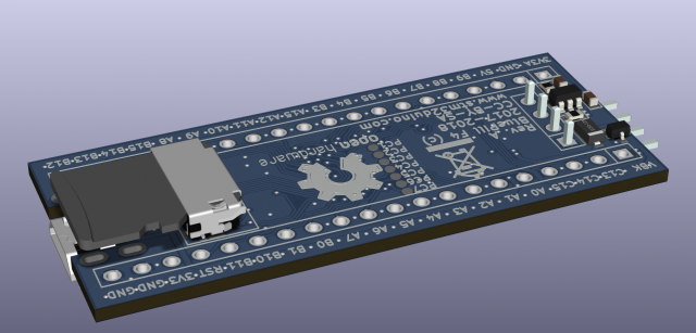
Now the card is oriented towards the outside, and it should be high enough to be inserted/removed with the plug attached. OTOH, the height below the PCB is 2.65 mm, i.e. a little bit taller than the pin header body (2.54 mm).
This connector has a mechanical card detect switch, but Chinese copies don’t necessarily feature it, so it is not connected, and anyway we have the SDIO_D3 trick to do the same electronically.
I’m downloading to see if I spot anything wrong.
Seems like you didn’t upload it yet. I had a quick look at the previous version anyway, and in the schematic the note on PC14 and PC15 “…shared with HSE…”, should read “…shared with LSE…” since those are for the low speed clock.
i like both options of sd card slots.
Unfortunatelly, I cannot keep traces for both solutions at the sme time, as all signals are mirrored. But is is still easy to reroute them without touching anything else if required, so I suggest to move along with this connector and use git to recover the previous solution if you need it.
I also cleaned up the traces.
I will not modify the board any more until I send it to allpcb.com, unless someone spots an error.
I will try to add the teardrops: I know how to do that in EagleCAD, but I never tried it in KiCAD. If someone has some experience, it is more than welcome…
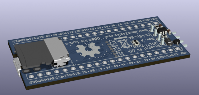
i’ll try to make some time tonight to have a look at the latest version.
I installed this KiCAD plugin, and here is the result: NOTHING HAPPENS
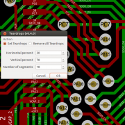
For installing plugins, I had to switch to the “nightly builds”, which breaks the schematic compatibility with older versions ![]() Typical free software bazaar
Typical free software bazaar ![]()
Now I will have to revert to the stable version for you guys to be able to work with the files I generate!
I know they are best practice for commercial boards, but for a few prototypes we can probably risk it without them.
I don’t normally use them, but I use larger vias , as I don’t normally need to design boards this compact
i like the battery connection part, and with the resistor to then connect the vbat to the 3v3
[RogerClark – Tue Jan 30, 2018 8:09 pm] –
How critical are teardrops?I know they are best practice for commercial boards, but for a few prototypes we can probably risk it without them.
I don’t normally use them, but I use larger vias , as I don’t normally need to design boards this compact
Teardrops are useful to get cheap PCB for mass production, with small vias like here (12 mils drill, 24 mils outer diameter). If the registration is off by 6 mils (not much…) near the via/trace junction, then you have no connection left…
I guess this is not too important for these prototypes, but I would really like to know how to do that in KiCAD, since I did it routinely under many other ECADs.
[racemaniac – Tue Jan 30, 2018 8:40 pm] –
didn’t have much time today, but had a quick look at the board, it’s looking good
i like the battery connection part, and with the resistor to then connect the vbat to the 3v3
Thanks, I tried to clean up traces as much as possible (less turns, shorter traces…).
I got the battery connection idea from Pito, the resistor is to get the compatibility with the “original” Bluepill when the charger is not mounted.
https://github.com/rustyoz/kicad/tree/teardrops
Video:
https://www.youtube.com/watch?v=Yu69JjOBIyY
Has anyone built Kicad from source before and feel like giving it a shot?
[victor_pv – Wed Jan 31, 2018 2:25 am] –
From some kicad developers mail list I fount this kicad branch which is supposed to include a menu to add teardrops:
https://github.com/rustyoz/kicad/tree/teardrops
Video:
https://www.youtube.com/watch?v=Yu69JjOBIyYHas anyone built Kicad from source before and feel like giving it a shot?
OK, I did:
sudo apt-get -y install libwxgtk3.0-0v5 libglew-dev libcairo2-dev libbz2-dev doxygen libssl-dev libboost-dev libboost-thread-dev libboost-context-dev libboost-filesystem-dev libboost-iostreams-dev libboost-locale-dev libboost-program-options-dev libboost-test-dev swig python-wxgtk3.0* git cmake libwxgtk3.0 libglm-dev libcurl3 libcurl3-dev python-dev

mkdir kicad

cd kicad/

mkdir build install

git clone -b teardrops https://github.com/rustyoz/kicad.git

cd build/

cmake -DCMAKE_BUILD_TYPE=Debug -DwxWidgets_USE_DEBUG=ON -DKICAD_SCRIPTING_WXPYTHON=ON -DKICAD_SCRIPTING=ON -DKICAD_SCRIPTING_MODULES=ON -DKICAD_SCRIPTING_ACTION_MENU=ON -DCMAKE_INSTALL_PREFIX=`<install_path>' ../kicad

make
The emails I found about that feature where from May last year. It seems like the owner of that repo merged the changes to the current code at the time so other people could test it, but there were no more emails, so seems like not a lot of people tested it
I’ll see if I can build it on Windows later, thanks for the notes on the errors, hopefully I’ll get it to compile too.
FYI, here is what I get using the standard EagleCAD “teardrops” ULP script on the same PCB:
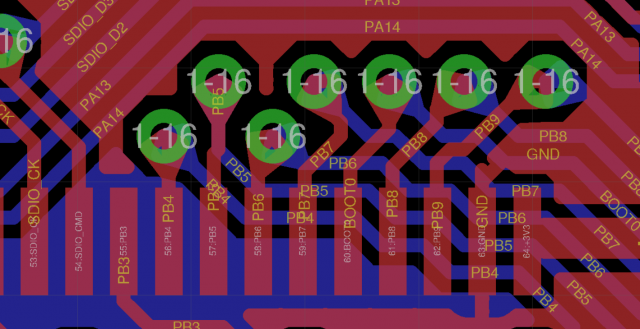
I left an issue to the author on Github.
Or that’s a different board that you have both in Eagle and Kicad?
Not too hard on such a small board, with all components on a 5 mil grid and traces on a 6 mil one. Once you get the traces in one, the other is easy to copy to using dual screens.
First conclusions:
- KiCAD teardrops are not functional
- drawing anything but copper traces is a pain (cannot edit but coordinates )
- … as is moving around blocks (possible, but only in OpenGL)
- laying out traces leaves a lot of poops everywhere, seems like it is magnetized on surrounding traces instead of the grid, bad when it is diagonal trace…
- 3D view is a must!
About kicad, one other very annoying issue I have found is that I move a component alone (without moving any traces) if any component pin ends up over a trace that belongs to another net, it will change the net of that trace to that of the pin/pad that landed over it. Pretty annoying when trying to place a component where some traces exist before moving them around. I don’t remember if it happens only in one of the modes (openGL or the other one), could be the case, but still I see no valid reason to have the net of a existing trace change just because some pad touched it.
We can skip the teardrops for the time being to start getting prototypes before CNY. I’ll check the current design in Kicad to see if I spot anything.
[victor_pv – Thu Feb 01, 2018 1:55 pm] – About kicad, one other very annoying issue I have found is that I move a component alone (without moving any traces) if any component pin ends up over a trace that belongs to another net, it will change the net of that trace to that of the pin/pad that landed over it. Pretty annoying when trying to place a component where some traces exist before moving them around. I don’t remember if it happens only in one of the modes (openGL or the other one), could be the case, but still I see no valid reason to have the net of a existing trace change just because some pad touched it.
Yes, I noticed it too. It looks like a trace has no signal, only pads, which is… weird! This is why you can have traces having their signal changed, or not having any signals on it either! Same reason too that you need a pad to have a ground stitching via, a simple “trace via” is not enough, since you cannot attach a signal to it!!! Just dumb IMHO.
[victor_pv – Thu Feb 01, 2018 1:55 pm] – We can skip the teardrops for the time being to start getting prototypes before CNY. I’ll check the current design in Kicad to see if I spot anything.
Yes, I think so, please check before we press the button!
Check slide 6:
http://instantdfm.bayareacircuits.com/d … k/results/
btw, does someone have some time to do a proper review?
i’ve got a bit of a cold atm, and just don’t have the attentionspan in the evening to properly look at it >_<
I could not see anything wrong on either. I would have perhaps added more gnd stitching in the area between NRST and PB1 pins in the header, and immediately below where the large GND PAD is, but likely not needed anyway.
I will take into account your remarks.
I found a strange issue, which is probably causing the gerber problems: all measurements (including min. trace width and clearance) have been truncated by a fly leg width: it looks like a rounding problem between imperial and metric system or something like that. Odd.
Unfortunatelly, it means that I have to change all trace widths on the PCB but also lay them again all one by one ![]()
I did it last evening for the top face, it takes quite some time to do it… I will perform the same healing operation tonight on the bottom face and we should be OK.
that’s an issue i wish upon nobody.
luckily while being a braindead monkeyjob, if you know how the traces should be, laying it out again isn’t that bad for a small board, but still
What I cannot explain is the origin of the problem: I started with a 6 mil width/clearance in Imperial units, I don’t know how it changed and if it will change again in the future.
[Squonk42 – Fri Feb 02, 2018 5:45 am] –
Unfortunatelly, it means that I have to change all trace widths on the PCB but also lay them again all one by oneI did it last evening for the top face, it takes quite some time to do it… I will perform the same healing operation tonight on the bottom face and we should be OK.
You can apply a new width to traces without having to lay them again.
Since I’m in the us I have mine set for imperial, and have not see that problem. I saw when I opened your files that trace widths had a lot of decimals, but I didn’t think anything of it. Perhaps internally does a conversion to imperial when it saves, then back to mm to display, and is loosing some decimals in each conversion?
Perhaps just setting that board to imperial may resolve that issue.
I tried several “light” methods without success. I can change all traces to 6 mils at once, but this doesn’t solve the clearance issue between traces, so the only way is to layout everything again. The board is not that big anyway, and it is a good opportunity to check ALL traces!
Please check everything as much as possible, it passes KiCAD DRC tool, but I don’t know if I can trust this one ![]()
Gerbers may need some cleanup, as there are silkscreen lines over some pads, but this is usually not an issue with PCB manufacturers, they trim it themselves.
Since it has an open end, I think it doesn’t help and may just act like an antenna, I think it would be better to move the vbk track up, so the ground fill ends under the vbk track where it just goes around the pins with no open end.
I can’t see anything that looks wrong.
Checked also the silk screens and seem fine to me.
This is how I think we could trace vbk to avoid the short length of gnd.
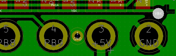
- bluepillf4.jpg (61.87 KiB) Viewed 249 times
[victor_pv – Sat Feb 03, 2018 2:07 pm] –
I was thinking SDIO_d0 and D1 could be rerouted to be shorter, by having their vias somewhere between PC7 and and PA8 vias, instead of routing above the PC7 vias, but then those 2 would be much shorter than the rest of the SDIO traces, and thought you probably did that routing in purpose to keep them all around the same lenght, is that right?
if that’s the case, is it worth it? max sdio frequency is 24Mhz, does the length difference really matter at that frequency?
And although we are “only” running @ 24 MHz, it does matter if you consider that the signal slopes are quite fast, meaning that you get all odd harmonics too… In the end, this brings more constant signal shapes between signals and better controlled skew.
I pushed a newer version where I fixed the “zone” minimum width and clearance values to 6 mils instead of 5.9753424324 ![]()
Here is the result on BayArea DFM:
http://instantdfm.bayareacircuits.com/d … v/results/
Looks like KiCad still does not compute clearance values the same way for filled areas ![]()
I tried to see if there was a way to reroute all SDIO tracks to keep them a bit shorter, but can’t get all of them, so your solution seems the only one to keep length the same.
There was some other rerouting I did it in around the top right corner of the MCU, but I had already messed up with the SDIO lines a lot, so I will see if I can do that again without touching the SDIO, it removed a via or two from a couple of GPIO lines.
EDIT: These are the ones, to PC6, PC7, Pb0 and PA6, removed a couple of vias and shortened the tracks a bit:
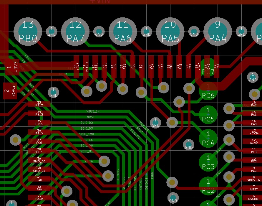
- bluepillf4-4.jpg (250.11 KiB) Viewed 211 times
[victor_pv – Sat Feb 03, 2018 3:17 pm] – I think we can pass with the 5.95, at least we can try.
I think these are really round-off errors, and AFAICT, these are taking place when traces are not colinear with the X or Y axis (ie. 45°). Probably not important.
[victor_pv – Sat Feb 03, 2018 3:17 pm] – I tried to see if there was a way to reroute all SDIO tracks to keep them a bit shorter, but can’t get all of them, so your solution seems the only one to keep length the same.
I tried many solutions, and this one seems the best, despite they make a “coil” pattern around the PC7 vias ![]()
If you find a better solution on a 6 mils grid, I take it!
[victor_pv – Sat Feb 03, 2018 3:17 pm] – There was some other rerouting I did it in around the top right corner of the MCU, but I had already messed up with the SDIO lines a lot, so I will see if I can do that again without touching the SDIO, it removed a via or two from a couple of GPIO lines.EDIT: These are the ones, to PC6, PC7, Pb0 and PA6, removed a couple of vias and shortened the tracks a bit:
I didn’t touch the SDIO lines, so those may be worth it.
I cannot get it with my 6 mils user grid: there is no grid line between the north STM32 pads and the north header row, so I cannot route PA6 and PB0 like you did. I think yours are probably off-grid, which I tried to avoid. So I don’t think I will include this change.
[victor_pv – Sat Feb 03, 2018 3:17 pm] – EDIT2:
I found a via that’s not needed right between PA1 and PA0 header pins, in +Vin trace. There is a via to switch from top to bottom, and then another that doesn’t switch sides, so I guess is a left over.
No, it is on purpose: when there is a power trace changing from one side to the other side of the PCB, I try to double the vias to double the via copper cylinder section for handling larger currents and reducing resistance.
Check this calculator:
http://circuitcalculator.com/wordpress/ … calculator
And this discussion on the EEVBlog:
https://www.eevblog.com/forum/manufactu … a-plating/
It is probably a little bit overkill here, since the maximum current will be 1A, but I have (bad?) habits ![]()
These 2 ones are not particularly close to each other, which kind of defeats the purpose. I pushed a new version where they are next to each other, and cleaned up a few others too.
[Squonk42 – Sat Feb 03, 2018 5:48 pm] –
No, it is on purpose: when there is a power trace changing from one side to the other side of the PCB, I try to double the vias to double the via copper cylinder section for handling larger currents and reducing resistance.
I think it cleaned the piece of trace between one via and the other when I selected the “Cleanup …” menu item, because there was only trace in one side when I looked at that, so the upper most via was not doing anything. I downloaded your files again and see the trace in both sides now, similar to the piece on the right of the NRST line (that one didn’t get messed up by the “cleanup” for some reason).
I was using a 2mil grid btw, so you are likely right that the same rerouting can’t be done with 6mil grid.
I can’t see anything wrong or anything else I would change.
Any other set of eyes to check it up?
While using 5mil grid, I can also route without vias PA12 PB3 and PB4:
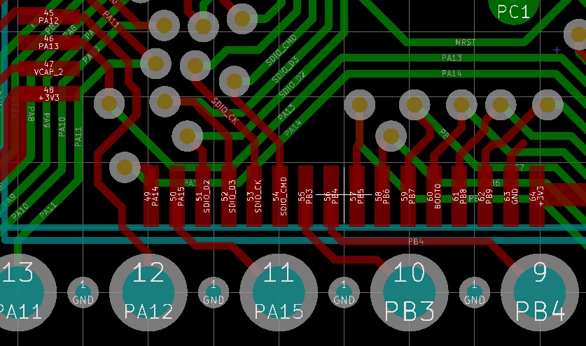
- bluepillf4-5.jpg (167.11 KiB) Viewed 231 times
The first grid makes SMT components (0805, 0603, 0402, 0201…) tile nicely on the board, the second grid is given by the manufacturing constraints, in our case, 6 mils trace width and spacing. This makes the routing most efficient, as traces will be separated by their minimum distance and on the grid.
I wish switching between these 2 grids could be made automatic…
[Squonk42 – Sun Feb 04, 2018 4:26 pm] –
I am using a 5 mils grid for component placement, and a 6 mils grid for trace routing.The first grid makes SMT components (0805, 0603, 0402, 0201…) tile nicely on the board, the second grid is given by the manufacturing constraints, in our case, 6 mils trace width and spacing. This makes the routing most efficient, as traces will be separated by their minimum distance and on the grid.
I wish switching between these 2 grids could be made automatic…
How do you select a grid size just for tracing? All I see in the top of my screen is 1 “Grid” dropdown, and doesn’t even give me the 6mil option, only 5 or 10.
Found the way, first define a user grid in the dimensions menu, then select the user grid in the drop down.
- STM32 F4 Assembly Top.pdf
- (33.63 KiB) Downloaded 41 times
[Squonk42 – Sun Feb 04, 2018 4:31 pm] –
Here are the Assembly drawings for top and bottom:
STM32 F4 Assembly Top.pdf
STM32 F4 Assembly Bottom.pdf
How did you get that? when I make the components values or reference visible, they are not within the footprint. Is that from the Eagle version?
This 2 kept getting flagged in bayarea DFM, so I added a keepout area for copper pour in the left (thin red rectangle), and move the track to overlap a bit more with the pour in the right, and they don’t get flagged anymore
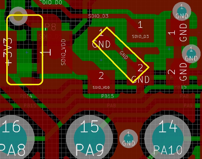
- bluepillf4-6.jpg (151.96 KiB) Viewed 213 times
I found another similar one between the 2 ground pads in the extreme right of your picture that was causing some concern to the BayArea DFM.
I pushed the new version to Github.
I tagged the version BluePill_F4_rev-A on Github.
Hopefully the PCBs will pass checks and get produced before Chinese New Year!

[Squonk42 – Mon Feb 05, 2018 5:05 pm] –
OK, 2x 40 boards ordered from AllPCB, one set by @victor_pv and one by me in blue solder mask, thickness 1.2 mm.I tagged the version BluePill_F4_rev-A on Github.
Hopefully the PCBs will pass checks and get produced before Chinese New Year!
I need a like button to like this post XD
EDIT:
- Fabricating.png (43.87 KiB) Viewed 252 times

- bluepillf4jpg.jpg (61.75 KiB) Viewed 245 times
- ALLPCB_Progress_1.png (38.07 KiB) Viewed 226 times
EDIT: Actually, if you take the existing “BluePillF4-F.Paste.gbr” file, it should be fine!
[Squonk42 – Tue Feb 06, 2018 12:26 pm] –
Thank you, I think I only need one stencil with all pads: even if I put solder paste in them but I don’t mount the component, at least it will protect the pads from oxidation. OK, I won’t include the board edge and I will do top side only, as the bottom side almost contains no component.EDIT: Actually, if you take the existing “BluePillF4-F.Paste.gbr” file, it should be fine!
Ok ![]()
i’ll try to remember to cut some stencils tonight, and then asap send them to you ![]()
*edit*
strange O_o’ i removed those pads from the paste layer, but when generating the paste gerber they’re still there o_O. must be missing something
I bought some solder paste ![]()
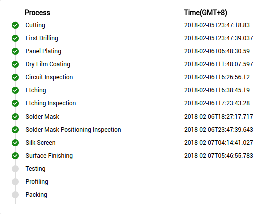
- ALLPCB_Progress_2.png (44.22 KiB) Viewed 194 times
- They are being produced side by side in the same lot
- They just bulk update times at once for multiple batches
- Somehow they found one the boards are the exact same and they are just producing 80 of them at once
Option 3 would be a surprise.
Strange that you cannot delete something you can see in KiCAD, though.
EDIT: I do have something too in BF.Pate, B.Paste, F.Mask and B.Mask layers, but they are immutable!!! Bug ![]()
I guess you have to edit the footprint file in a text editor to remove them. ![]()
Anyway, I am not impressed at all by the drawing facilities outside copper layers in KiCAD: basically, you have to use an external tool to generate your drawings and import them into KiCAD, as the available tools are just a misery.
BTW, here is the PCB status:
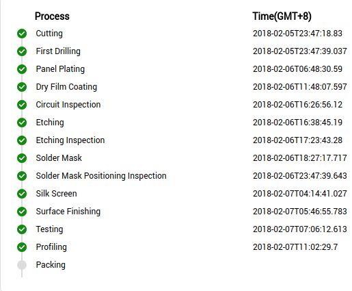
- ALLPCB_Progress_3.png (47.8 KiB) Viewed 461 times
[Squonk42 – Wed Feb 07, 2018 7:31 am] –
I probably did the footprint in EagleCAD then, and imported it in KiCAD.Strange that you cannot delete something you can see in KiCAD, though.
EDIT: I do have something too in BF.Pate, B.Paste, F.Mask and B.Mask layers, but they are immutable!!! Bug
I guess you have to edit the footprint file in a text editor to remove them.
Anyway, I am not impressed at all by the drawing facilities outside copper layers in KiCAD: basically, you have to use an external tool to generate your drawings and import them into KiCAD, as the available tools are just a misery.
BTW, here is the PCB status:
ALLPCB_Progress_3.pngAlmost done!
yup, ended up removing them manually. and indeed, besides copper all you can do is import it via the tool, can’t say i missed it, but can imagine it can be useful.
cutting stencils as we speak, they’ll probably be mailed tomorrow (don’t have time to do so today)
All the crystals I find in that size have 4 pins.
Did anyone find it on Mouser?
It is available on Digi-Key, though.
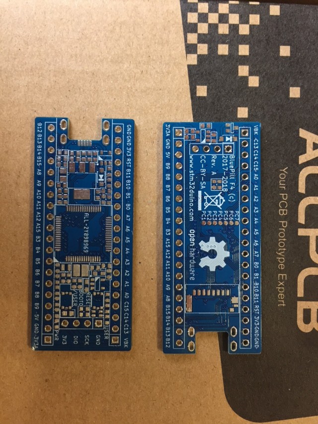
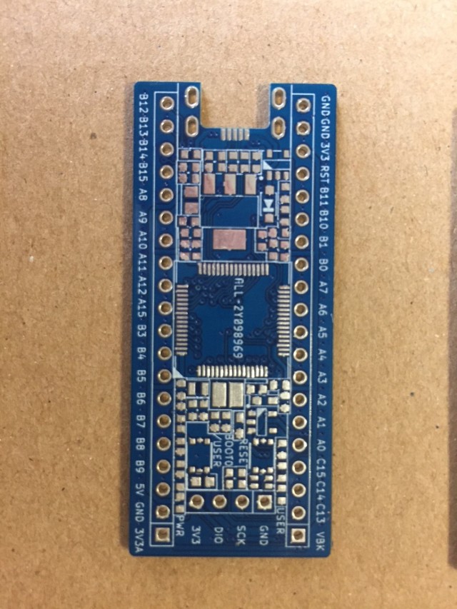
that was fast
i hope the stencils i sent also arrive soon ^^
Mine were in Ohio this morning, but expected delivery by EOD today.
I was trying to find the couple of components I need in digikey since Mouser doesn’t have the right Crystal, and mouser doesn’t have the regulator in stock(and minimum order qty. 4000), and noticed the regulator we are using, the AP2214HA is not pin compatible with the AMS1117. Not sure if was intentional, but there is the 2114H version that’s pin compatible with the ams1117 of which I have a bunch.
If you ar eordering some parts at Digi-Key, I may be interested in some (I don’t have the 1616 RGB LED) if you can forward them to me, as they don’t provide USPS to EU so shipping from them is expensive. Things like crystals (I have a few), F405 (I only have 2) and AP2214HA (I only have 5).
That would require to change the PLL divider, but other than that should work for everything according to the cubemx clock tool.
I was going to order a couple of those while the others from china arrive. It may be good to switch to 4pin crystals in the next iteration if they are the same price in china as the NX3225GD, since finding them in the US is way easier.
One things I noticed, while finding the crystal caps, is the crystal shows a CL of 8pF (both the right part number in digikey, as the 16Mhz compatible I found), but in the schematic we are using 20pF caps. Shouldn’t we be using a lower value?
I’ll be order a couple of MCUs, an F103 and an F405. i have a few more in order from China, and when checking 64pin MCUs in mouser, I found the 722RET6 is about the same price as the 405RGT, then did a search in Ali (no good) and ebay (bingo), so I have ordered this:
https://www.ebay.com/itm/5pcs-STM32F722 … Sw8A1aeDF3
Only a couple of pins are different, and mainly we lose PB11, but I think is a low price to pay for having an F7 bluepill.
I will be placing an order from Mouser today (only they have the AP2114HA-3.3), and try to order all I need from them, mainly the ldo, xtal, xtal caps, battery changer, and fet. let me know what parts you want.
CL is a serial combination of the 2 capacitors – 20pF ser 20pF is 10pF which is the ~same value as the 8pF..
2x18pF would give you 9pF.. But with pF values and tolerances of the ceramics it does not matter basically..
And then I understand there is the residual capacitance in the circuit, which add to the capacitors, so depending on that the capacitors may need to be a bit smaller.
Here is a very interesting Application Note from ST.
In particular, in section 3.3:
CL = (CL1 * CL2) / (CL1 + CL2) - Cs
Also, it needs a different windows driver ( I forget which one), which needs to be installed by Zadig..
There is a separate thread about the F4 bootloader, but I can’t find it at the moment.
In that thread, there is also a software version of the same bootloader, ( which used DFUSe) , which may be more useful if the Core can automatically reset and then run the bootloader
However the bootloader is not clever like the F1 bootloader and it does not have a timeout , for normal startup, when the IDE is not about to upload …
I think a better option in the medium term, is to try to port the existing F1 bootloader to the F4.
I found some sites in China which claim to have ported the F1 bootloader to the F4, but I think you have to buy the code, and I am not even sure the sites work at all, even if someone e.g. in China could pay the few dollars for the code…
So we will probably need to port the code ourselves..
Re:Core
STM32GENERIC may be the best option, because although the LibMaple F4 Core has the basic functionality, it does not have a lot of the advanced features like SDIO
[RogerClark – Sat Feb 10, 2018 10:16 pm] –
Re:CoreSTM32GENERIC may be the best option, because although the LibMaple F4 Core has the basic functionality, it does not have a lot of the advanced features like SDIO
Well, according to the info here, the Arduino_STM32 core supports a lot of F4 stuff, including SDIO.
I think Victor added SIO recently.
But here are many things missing from the F4 version of the LibMaple F4 (Arduino_STM32)
BTW.
I agree… Just use STLink to upload.
I ported Steve’s to libmaple F1.
About bootloader, I started the thread with the F4 bootloader, it was based an STM application note.
Adding the timeout should be easy enough. Making it compatible with the F1 may not be so easy, but honestly as long as we may reliably launch dfuse from the IDE and the bootloader reboots after a reasonable timeout, I think that would not matter.
The bootloader is independent what core we use.
I think give the effort STM in putting in their core, and that’s highly portable to more MCU, I plan to give it a shot.
[Squonk42 – Sat Feb 10, 2018 8:31 am] –
If you ar eordering some parts at Digi-Key, I may be interested in some (I don’t have the 1616 RGB LED) if you can forward them to me, as they don’t provide USPS to EU so shipping from them is expensive. Things like crystals (I have a few), F405 (I only have 2) and AP2214HA (I only have 5).
I still haven’t place my order, but need to do so by tomorrow, which components do you need?
[RogerClark – Sat Feb 10, 2018 10:54 pm] –
SteveI think Victor added SIO recently.
But here are many things missing from the F4 version of the LibMaple F4 (Arduino_STM32)
BTW.
I agree… Just use STLink to upload.
Yes, on the STM32F405, the USB DFU mode requires the HSE external crystal, which may not work for us in the early stages, see ST AN2606, page 97.
[Squonk42 – Sun Feb 11, 2018 10:15 am] –[RogerClark – Sat Feb 10, 2018 10:54 pm] –
SteveI think Victor added SIO recently.
But here are many things missing from the F4 version of the LibMaple F4 (Arduino_STM32)
BTW.
I agree… Just use STLink to upload.
Yes, on the STM32F405, the USB DFU mode requires the HSE external crystal, which may not work for us in the early stages, see ST AN2606, page 97.
?? Is there not 8M HSE external crystal on BP F4 board?
It is easy to upload STM32F4 on Arduino IDE by USB DFU mode if you don’t mind to hold BOOT0 and press nRST key at everytime upload. I’ve tested on STM32F401.
but I think it is stupid press any keys before upload.
I Still have not better way to upload STM32F4 base on ST official bootloader.
[csnol – Sun Feb 11, 2018 2:15 pm] –[Squonk42 – Sun Feb 11, 2018 10:15 am] –[RogerClark – Sat Feb 10, 2018 10:54 pm] –
SteveI think Victor added SIO recently.
But here are many things missing from the F4 version of the LibMaple F4 (Arduino_STM32)
BTW.
I agree… Just use STLink to upload.
Yes, on the STM32F405, the USB DFU mode requires the HSE external crystal, which may not work for us in the early stages, see ST AN2606, page 97.
?? Is there not 8M HSE external crystal on BP F4 board?
It is easy to upload STM32F4 on Arduino IDE by USB DFU mode if you don’t mind to hold BOOT0 and press nRST key at everytime upload. I’ve tested on STM32F401.
but I think it is stupid press any keys before upload.
I Still have not better way to upload STM32F4 base on ST official bootloader.
…
follow the discussion a bit before you panic ![]() . We’re going to slowly test the features of this board, not just slap everything on and pray it works. That includes things like the crystals. Step by step verify subparts working. So once we come to mounting the crystals, we can start using the bootloader etc… but that’s not our first priority.
. We’re going to slowly test the features of this board, not just slap everything on and pray it works. That includes things like the crystals. Step by step verify subparts working. So once we come to mounting the crystals, we can start using the bootloader etc… but that’s not our first priority.
[victor_pv – Sun Feb 11, 2018 5:56 am] –[Squonk42 – Sat Feb 10, 2018 8:31 am] –
If you ar eordering some parts at Digi-Key, I may be interested in some (I don’t have the 1616 RGB LED) if you can forward them to me, as they don’t provide USPS to EU so shipping from them is expensive. Things like crystals (I have a few), F405 (I only have 2) and AP2214HA (I only have 5).I still haven’t place my order, but need to do so by tomorrow, which components do you need?
Well, I have most of the parts for non-optional features, except for the 1616 RGB LED (D2) and some stupid 510R and 560R resistors (R2/R3/R12/R14) but I should be able to get these last ones.
However, I only have 2x STM32F405RGT6 (U3) and only 5x AP2114HA (U1) and 5x FC-12M crystals (Y1).
And I don’t have the parts for the battery charger: MCP73812T-320I/OT (U5), IRLML6402 (Q1) and 15k resistor (R17).
If you can get some extra of these in the same shipping from Mouser/DK (at least the ones I am missing or having in QTY < 5), please drop them in an envelope and send them to me by USPS, I will refund you via PP if you don’t mind.
I have 10x NX3225GD (Y2), 20x SY6280 (U4) and 50x micro USB connectors (J5) that perfectly fit into the footprint (yeah!), so if you need some, pelase let me know!
SDIO seems to work really well too – with the right cards.
I’ve not noticed much activity from Daniel lately, has he ‘moved on’?
- U1/C6/C8/C18 for the main LDO
- U2/C1/C7/L2 for the analog LDO
- D1/R2 for the power LED (I had to change R2 to 150R instead of 510R)
- R19/R20 to bypass the charger
- J5/D3 to feed +5V from USB
I have +4.84V on the 5V pins (because of the D3 Schottky diode drop), supplied by a wall wart (I don’t have a bench supply and I don’t want to fry my PC ![]() ).
).
The 3V3 is a little low at +3.20V, but the 3V3A OTOH is rather high at +4.20V ?!? No detected heat on any component. I checked with a scope and all voltages look clean. All other header pins are at 0V, and the green POWER LED turns on.
I checked U2 (the AP2112K3.3-TRG1 LDO), it is marked “G3P” which matches the datasheet. Its VIN pin is at 4.84V as well as its EN pin, GND is at 0V, but VOUT is +4.20V ![]()
I will check the solder joints tomorrow at work with a Mantis binocular to see if there is something wrong.
Any idea?
The AP2112 doesn’t appear to come in a 4.2V version, so it isn’t a packaging mistake. I suppose it could possibly be a fake.
I don’t know for the AP2112, but a fake is a possibility, I bought them from AliExpress…
[Squonk42 – Sun Feb 11, 2018 3:43 pm] –
If you can get some extra of these in the same shipping from Mouser/DK (at least the ones I am missing or having in QTY < 5), please drop them in an envelope and send them to me by USPS, I will refund you via PP if you don’t mind.I have 10x NX3225GD (Y2), 20x SY6280 (U4) and 50x micro USB connectors (J5) that perfectly fit into the footprint (yeah!), so if you need some, pelase let me know!
Send me a private with the quantities you want of each part and I’ll add to my order.
1) The GND pin on the regulator is floating (caused by a bad or missing track, via etc)
2) The regulator is in back to front and we are getting a diode drop or something rather than regulation.
3) There is a path to 5V via a diode (or some other semiconductor junction(s)) from the output of the regulator.
[ahull – Sun Feb 11, 2018 10:09 pm] –
Some of other possibilities in order of likely hood.1) The GND pin on the regulator is floating (caused by a bad or missing track, via etc)
2) The regulator is in back to front and we are getting a diode drop or something rather than regulation.
3) There is a path to 5V via a diode (or some other semiconductor junction(s)) from the output of the regulator.
There is what is supposed to be (you never know with Aliexpress…) a ferrite bead between GND and AGND, I will check it for 1)
[Squonk42 – Mon Feb 12, 2018 5:38 am] –[ahull – Sun Feb 11, 2018 10:09 pm] –
Some of other possibilities in order of likely hood.1) The GND pin on the regulator is floating (caused by a bad or missing track, via etc)
2) The regulator is in back to front and we are getting a diode drop or something rather than regulation.
3) There is a path to 5V via a diode (or some other semiconductor junction(s)) from the output of the regulator.There is what is supposed to be (you never know with Aliexpress…) a ferrite bead between GND and AGND, I will check it for 1)
OK, it is a ferrite bead indeed, but the solder joint was bad ![]() : I got a steady +3.30V on digital 3V3 and +3.29V on 3V3A, yeah!
: I got a steady +3.30V on digital 3V3 and +3.29V on 3V3A, yeah!
Next step: add the tactile switches for USER/BOOT0 and RESET with all related parts, pull-down on BOOT1, decoupling capacitor on SWD and a single LED on PC13 as I don’t have yet an 1616 RGB LED, all of these are low-risk, but easier to test without the STM32F405 installed.
Then mount the USB power Switch U4 (SY6280) and check if it controls VBUS by toggling its VBUS_EN input and check if the VBUS=>+5V Schottky diode is also working as expected.
[RogerClark – Mon Feb 12, 2018 9:49 pm] –
Nice catch Andy…. even though you don’t have the PCB
?!?
I thought the problem was related to one of the things Andy suggested.
[RogerClark – Tue Feb 13, 2018 10:53 am] –
My misunderstandingI thought the problem was related to one of the things Andy suggested.
Wasn’t andy right? due to the badly soldered ferrite bead, the GND was indeed floating causing the issue ![]()
but of course also good catch of squonk to spot his bad soldering ^^

Of course he was right!
I found a schematic bug on the RESET button: the NRST is active low… It should be connected to the R6 pull-up by default, and not to the C15 debounce capacitor, i.e. to the pin 1 or 3 of tactile switch S2, not to pin 2 or 4!
Otherwise, a single red led fitted in the 1616 RGB footprint, mounted with R3 only (R14/R15 not mounted) works as expected, i.e. like the single LED on PC13 from he original BluePill. I lowered R3 to 150R because I had no 510R on hand, but both value may work, just no as bright.
R1 pull-down resistor on PB2 (BOOT1) is OK, as well as BOOT0/USER button and connection to PB8 is also OK.
Next step (maybe not tonight!) is to test the USB load switch U4 and the Schottky diode D3, then mount the decoupling capacitors and the STM32F405 itself and make the LED blink!
Then the 2x crystals one by one, and test the SD Card. Battery charger option is last in my list, as I don’t have the parts yet).
[Squonk42 – Wed Feb 14, 2018 10:50 am] – I found a schematic bug on the RESET button: the NRST is active low… It should be connected to the R6 pull-up by default, and not to the C15 debounce capacitor, i.e. to the pin 1 or 3 of tactile switch S2, not to pin 2 or 4!
Simplest fix: cut the NRST trace on the bottom face just before the via under the RESET tactile switch and add a wire on top face between R6 pad 2 and the NRST header pin.
If this is meant something cheap & easy to produce, i think those ground pads are just too dangerous to leave there (and they don’t really serve any use anyway i think?)
I soldered the USB load switch and related components, but I had no time yet to test it and the Schottky diode.
What I have left to solder and test are the CPU with all its decoupling capacitors, then the 2 crystals and capacitors, the SDIO Card connector and decoupling, and the optional battery charger circuit.
Apart from my bad solder joint above and the wrong polarity for the RESET button, nothing else to report for the moment.
Other than the track we need to cut and watching out for shorts under the buttons, anything else so far?
Good news from my board: just made contact to it via st link
(and due to a lack of ferrite beads, i replaced them by a piece of wire ^^)
Very good if it is responding the STLink!
Did you take into account my remark regarding the crystal capacitors that were swapped? It will probably be the most tricky part to adjust if we want to have the crystals starting reliably.
[Squonk42 – Sat Feb 17, 2018 10:54 am] –
No, nothing else.Very good if it is responding the STLink!
Did you take into account my remark regarding the crystal capacitors that were swapped? It will probably be the most tricky part to adjust if we want to have the crystals starting reliably.
nope, haven’t taken that into account yet, and indeed, swapping them won’t be easy ^^’
i’ll see what i can do to get around it
– swapped crystal capacitors
– reset button
– button ground pads
[Squonk42 – Sat Feb 17, 2018 12:37 pm] –
Dual soldering iron
ow, just saw it’s just the caps that are switched, shouldn’t be hard to fix with my hot air station ![]()
*edit* swapped them ^^
really glad i have a hot air station, a cheap aoyue one already goes a long way when working on such pcb’s ![]()
- Do not mount R6, it is not required anyway, since the STM32 features an internal 30~50k pull-up resistor
- put a nice solder blob between R6 pad 2 and nearby C15 pad 1 (GND)
This is equivalent to this circuit from the datasheet:
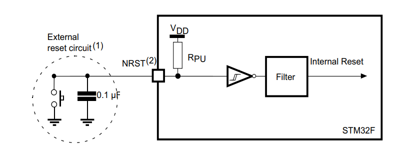
- NRST.png (25.25 KiB) Viewed 272 times
i can program the stm32, but can’t get the blink working, wondering if i made some stupid mistake >_< (i hope i didn’t damage the mcu)
I think perhaps STLink can upload even if the clock is not running
If the STM32 is still responsive to the JLink, it is not fried yet ![]()
but i’ll see if i can do some SWD debugging to see if i can find a reason it’s not starting the blink program >_<
[Squonk42 – Sun Feb 18, 2018 8:22 am] –
Ideas: reverse the LeD
thanks for the vote of confidence :p
already checked all electrical things, it’s not that, probably just something going wrong with the program i generated via cubemx
Do you have a known-working STM32F4xx board (STM32F4DISCOVERY)?
[Squonk42 – Sun Feb 18, 2018 10:15 am] –
Haha, I was joking!Do you have a known-working STM32F4xx board (STM32F4DISCOVERY)?
maybe, not sure, i’ll have a look in my big drawer of boards XD
*edit*
found a 407 board, should be close enough i hope ![]()
They look very nice
I’ve been slowly receiving parts from China and hope to get some more from Mouser tomorrow or Tuesday.
There are no obvious shorts on the board (visual inspection and minimal measurement).
I don’t think I will have the digital regulator parts, so my current plan is to install a processor – probably the SM32F411 (I also got a STM32L496RGT6 and a STM32L462RET6 — I want to play with the Single Wire Protocol interface on PB12).
I have some CubeMX code to test all the GPIO pins on the header connection with one of those 6 bit Arduino led modules. I’ve tested it on a bluepill and a F407 board I have. It uses the internally generated clock to avoid worrying about the oscillators at first. I’ll probably power it over the SWD interface or lab power supply directly to the 3V3 input.
I’ll be programming with a Baites ST-Link and BMP software.
Not sure what will be next to test after that. It might be time to get some CubeMX SDIO experience!
BTW what is the planned core to try developing for these boards?
Eric
I found out I didn’t have any ferrites because an order I placed a while back with some was wrong, so I had to use 0R in place of all ferrites.
I also didn’t have enought 10uF capacitors to reflow more than 2 boards for the same reason. I was going to reflow more boards at once, but given that I had to sub several components, I decided to hold until I get the right components to reflow more.
Power on test went fine, power led lights up, and I measure 3.27V and 3V29 in those boards in 3v3 and 3v3a
These 2 boards will get F103RCT MCUs. I’ll place an order to digikey for the components I found I’m missing and reflow another couple next week for F4 mcus.
In the meanwhile if any of these 2 work right with an F103 I can start testing oscillator, pins, usb etc.
EDIT: about the core, there are some mentions above. The libmaple F4 core should work with some modification depending on the MCU you use, but I think the STM32Generic from Danieleff and the official STM core are likely the best going forward. The libmaple one definitely works in F407 boards.
[Pito – Mon Feb 19, 2018 11:12 am] –
Is there any list of mcus which fit onto the board (without any mods)?
we should make a list, but when discussed earlier, i think the conclusion was that almost all 64 pin mcu’s are compatible (with the only differences being the 103’s requiring a 0R resistor where the others require the VCAP 2.2uF capacitors)
[Pito – Mon Feb 19, 2018 11:12 am] –
Is there any list of mcus which fit onto the board (without any mods)?
From my previous post 45 pages ago:
STM32L052R6 STM32L052R8 STM32L053R6 STM32L053R8 STM32L063R8 STM32L072RB STM32L072RZ STM32L073RB STM32L073RZ STM32L083RZ STM32L100R8 STM32L100R8-A STM32L100RB STM32L100RB-A STM32L100RC STM32L151R6 STM32L151R6-A STM32L151R8 STM32L151R8-A STM32L151RB STM32L151RB-A STM32L151RC STM32L151RC-A STM32L151RD STM32L151RE STM32L152R6 STM32L152R6-A STM32L152R8 STM32L152R8-A STM32L152RB STM32L152RB-A STM32L152RC STM32L152RC-A STM32L152RD STM32L152RE STM32L162RC STM32L162RC-A STM32L162RD STM32L162RE STM32L433RB STM32L433RC STM32L443RC STM32L452RC STM32L452RE STM32L462RE STM32F070RB STM32F072R8 STM32F072RB STM32F078RB STM32F102R4 STM32F102R6 STM32F102R8 STM32F102RB STM32F103R4 STM32F103R6 STM32F103R8 STM32F103RB STM32F103RC STM32F103RD STM32F103RE STM32F103RF STM32F103RG STM32F302R6 STM32F302R8 STM32F302RB STM32F302RC STM32F302RD STM32F302RE STM32F303R6 STM32F303R8 STM32F303RB STM32F303RC STM32F303RD STM32F303RE STM32F373R8 STM32F373RB STM32F373RC
And as @racemaniac said, there is a BOM change between F1 and F4 (0R vs. VCAP on 2 pins).
F722 datasheet
from what I have seen:
- F405: Assemble all components as listed, including the 2×2.2uF capacitors
- F103: Replace both 2.2uF capacitors with 0R resistors
- F4x1: Replace the capacitor going to vcap_1 with 0R. Loses pin PB11 in the header, which should connect to a capacitor instead (small modification adding a TH cap, but no need to cut tracks). PC5 pad becomes PB0, PB0 is PB1, PB1 is PB2, and a couple others I can’t remember.
- F722: Similar to F4x1, but also some pins change names (small modification and pin names don’t match for those pins, but again no need to cut tracks
If anyone has time to write a more detail table on what to populate or leave empty when using the following, we can open a new thread about assembly of the boards with all the details in the first post.
Assembly options:
- R405 MCU
- R4x1 – 4×0 MCU
- F103 MCU
- F722 MCU
- … Other MCU options.
- Option with FB/2112 for VDDA
- Option for charger/no charger
- Option for RGB/Normal led
- Option for Boot1 button to also be user button
- Option for no power led (saves power)
[Squonk42 – Wed Dec 13, 2017 8:56 pm] –
There still might be some changes, I just received the micro USB connectors from AliExpress today, and they don’t match exactly the Molex 47642-0001 footprint: the rear “hook” pins are closer to the PCB edge by 1 mm
However, it perfectly matches the one on the original Bluepill! I asked the vendor for a drawing, and will modify the footprint to be compatible with both.
I will share the Kicad files are soon as they are stable enough (hopefully before the end of this WE), before adding any option.
I mentioned this in the PM, but to give more details and for everyone else to know.
I ordered a couple of Molex 47642-0001 for first boards. Yesterday during assembly I found out the hooks are a bit more separated than the holes in the PCB allow, so it’s not a good fit for the current footprint.
The width is right, but lengthwise they are about .5mm further apart. I had to cut off the front two hooks. I could have cut off the back ones, either way would have worked. The usb lines pads are longer than the tiny pins in the connector, so enlarging the front hooks forward, or enlarging the rear hooks backups would still allow contact of the pins with the pads.
The width, so the hook distance left to right was fine.
[victor_pv – Mon Feb 19, 2018 1:59 pm] –
Assembly options:
- R405 MCU
- R4x1 – 4×0 MCU
- F103 MCU
- F722 MCU
- … Other MCU options.
- Option with FB/2112 for VDDA
- Option for charger/no charger
- RGB LED or normal LED
Thinking about the user button, I have a concern on R5 being 0R. If it’s populated and an unaware user connects PB8 to GND for whatever reason in his circuit, or drives PB8 down for some use, and then press the button, it can cause a short.
Imagine a case where he chooses to use PB8 as the CS pin for something, so it’s driven down in the sketch when using whatever peripheral.
At the same time, he intends to reset the board, but by mistake presses the user button, which causes a short between a low PB8 and 3V3.
Wouldn’t be it as useful if we used 1K for R5? it would still be a strong pull up in PB8 vs the 100K pullup, but would remove the posibility of a short. The maximum current would be 3.3mA to PB8 which is within spec. Even a 2k2 resistor would still be strong enough vs the 100K pulldown.
EDIT:
Some progress with my boards. I soldered an STM32F103RCT6 to one of them. Next recompiled the bootloader for 16Mhz xtal (I got a couple from mouser since they didn’t have the 8Mhz ones).
The bootloader works fine, so next I modified the core to support 16Mhz crystals (added a new HSE option to enable HSE_DIV_2, so the 16Mhz get divided to 8Mhz before going to the PLL), and uploaded a blink sketch, and that works fine.
So far then the USB peripheral is working, the oscillator with a 16Mhz crystal is working, and PC13 and the LED are working.
Next will be the button in PB8 (so far it doesn’t work in the bootloader, but perhaps I overlooked something).
This board doesn’t have an RGB led, so I may solder that to the other one I reflowed.
[victor_pv – Mon Feb 19, 2018 1:59 pm] –
- F4x1: Replace the capacitor going to vcap_1 with 0R. Loses pin PB11 in the header, which should connect to a capacitor instead (small modification adding a TH cap, but no need to cut tracks). PC5 pad becomes PB0, PB0 is PB1, PB1 is PB2, and a couple others I can’t remember.
- F722: Similar to F4x1, but also some pins change names (small modification and pin names don’t match for those pins, but again no need to cut tracks
Victor
I think you’ve got confused with the F411 pins. I found it tricky to keep track with 5 pdfs open at once ![]()
I think the non-power related pins are all the same on all the devices apart from the F722 which seems to drop PC5 instead of PB11 like the other chips. It also offsets the pins for PB0,1,2,10 and 11.
For the LQFP64 packages:
Pin    F103     F405     F411     L462     F722

46     VSS_1    VCAP_2   VSS      VSS      VSS

31     VSS_2    VCAP_1   VSS      VSS      VSS

30     PB11     PB11     VCAP_1   PB11     VCAP_1

29     PB10     PB10     PB10     PB10     PB11
[victor_pv – Mon Feb 19, 2018 5:33 pm] –
I updated the list.
Thinking about the user button, I have a concern on R5 being 0R. If it’s populated and an unaware user connects PB8 to GND for whatever reason in his circuit, or drives PB8 down for some use, and then press the button, it can cause a short.
Imagine a case where he chooses to use PB8 as the CS pin for something, so it’s driven down in the sketch when using whatever peripheral.
At the same time, he intends to reset the board, but by mistake presses the user button, which causes a short between a low PB8 and 3V3.Wouldn’t be it as useful if we used 1K for R5? it would still be a strong pull up in PB8 vs the 100K pullup, but would remove the posibility of a short. The maximum current would be 3.3mA to PB8 which is within spec. Even a 2k2 resistor would still be strong enough vs the 100K pulldown.
Yes, you are probably right, better use a small value resistor to avoid a short.
[victor_pv – Mon Feb 19, 2018 5:33 pm] –
EDIT:
Some progress with my boards. I soldered an STM32F103RCT6 to one of them. Next recompiled the bootloader for 16Mhz xtal (I got a couple from mouser since they didn’t have the 8Mhz ones).
The bootloader works fine, so next I modified the core to support 16Mhz crystals (added a new HSE option to enable HSE_DIV_2, so the 16Mhz get divided to 8Mhz before going to the PLL), and uploaded a blink sketch, and that works fine.
So far then the USB peripheral is working, the oscillator with a 16Mhz crystal is working, and PC13 and the LED are working.
Next will be the button in PB8 (so far it doesn’t work in the bootloader, but perhaps I overlooked something).This board doesn’t have an RGB led, so I may solder that to the other one I reflowed.
OK, good, if the USB peripheral, the HSE crystal and the single LED are all working with an STM32F103RCT6, there is a good chance that it will also work with the STM32F405 too!
I wanted to check electrically the USB load switch and Schottky diode between VUSB and +5V before mounting a CPU, but I don’t have much time currently to work on it.
Then, I wonder if it is better to solder an F103 or an F405 first on my board.
-The F103 has mature core with plenty of libraries, sketches etc, and I know how everything works better than the F4.
-The MCU is half the price, so if I burn 1 it won’t hurt as much.
So far I tested the button with a 2k resistor, and works just fine.
I believe I may have installed the wrong I limiter resistor for the SY, I need to check, but at least it’s all powering up at the moment.
Working for me so far:
- 16Mhz clock (I’ll check and publish the value of my caps, believe was 6p8 or 4p7)
- USB port
- USB power
- PC13 led (red, 1K resistor)
- PB8 button (with 2k rather than 0R)
To test:
- 32Khz clock
- Some other pins
- sd once I get the sd card slot.
Concerns I have at the moment:
Ferrite bead in analog ground. I know there was some discussion, but I thought adding a ferrite bead in the AGND will isolate the high frequency noise in the MCU side, which is not what we want. I have read all I could find about the subject, and seems like that would only make sense if whatever analog signal we measure uses the same ground as AGND, and then an FB separating those from the other ground.
But in our case AGND is not available in the pin headers, so anything we want to measure with the analog pins will take the ground from the common ground, so we are not filtering all analog ground from the rest, but separate the analog ground in the MCU from the analog ground in anything analog we measure, and that would make the high frequencies ground float inside the MCU.
[victor_pv – Tue Feb 20, 2018 3:55 pm] –
I started with the F103 for 2 reasons:
-The F103 has mature code with plenty of libraries, sketches etc, and I know how everything works better than the F4.
-The MCU is half the price, so if I burn 1 it won’t hurt as much.So far I tested the button with a 2k resistor, and works just fine.
I believe I may have installed the wrong I limiter resistor for the SY, I need to check, but at least it’s all powering up at the moment.Working for me so far:
- 16Mhz clock (I’ll check and publish the value of my caps, believe was 6p8 or 4p7)
- USB port
- USB power
- PC13 led (red, 1K resistor)
- PB8 button (with 2k rather than 0R)
To test:
- 32Khz clock
- Some other pins
- sd once I get the sd card slot.
Concerns I have at the moment:
Ferrite bead in analog ground. I know there was some discussion, but I thought adding a ferrite bead in the AGND will isolate the high frequency noise in the MCU side, which is not what we want. I have read all I could find about the subject, and seems like that would only make sense if whatever analog signal we measure uses the same ground as AGND, and then an FB separating those from the other ground.
But in our case AGND is not available in the pin headers, so anything we want to measure with the analog pins will take the ground from the common ground, so we are not filtering all analog ground from the rest, but separate the analog ground in the MCU from the analog ground in anything analog we measure, and that would make the high frequencies ground float inside the MCU.
I can’t check right now, but isn’t one of the grounds exposed the agnd? (i thought it was one of the compromises towards backwards compatibility we made)
[racemaniac – Tue Feb 20, 2018 4:01 pm] –
I can’t check right now, but isn’t one of the grounds exposed the agnd? (i thought it was one of the compromises towards backwards compatibility we made)
Nothing is labelled as AGND in the board, but I can’t check the schematic to confirm right now.
Which means that the ferrite bead between GND and AGND is useless IMHO.
And if the passive PI filter between +3V3 and +3V3A is working as expected (to be tested), we should get the same PSRR as the AP2112 Analog LDO.
viewtopic.php?f=19&t=2633&p=37893&hilit=ferrite#p37893
I think in that case it’s safe to just replace the AGND FB with a 0R or a solder bridge, and may even help to keep noise under control.
I would suggest to make some practical measurements – with 0ohm and with FB.
The topic is pretty tricky, so better do make measurements (various FB values) and compare on your first release pcb, rather than throwing FBs out in the next pcb release.
Also mind FBs need some ceramics at each side (Pi), 100nF is too much, 1-10nF closest to the FB, then you may continue with 100nF etc.
In order to filter everything reasonable out the Analog Devices guys (they know well) recommend 1nF||100nF||10uF everywhere (there is an app note somewhere on it). That is not easy to do with current pcb unless you go 0402 or less.
Also keep track on all the issues found and lessons learned, best in one place (ie a separate topic).
I have installed:
- Switches — found those a bit tricky to do. Reset and Boot0 are operating correctly.
- RGB LED / Power LED and resistors
- STM32L462 and associated resistors and capacitors
- NRST fix
- SWD header
I was able to successfully program it to cycle through all 8 options on the RGB LED ![]()
This was very satisfying since I thought I’d fried the MCU during soldering.
I wrote the code in CubeMX and used the internal oscillator.
It was clearly silly to start with this uncommon processor — my BMP didn’t recognise it and this reinforced my belief that is was dead.
Similarly openocd wasn’t letting my connect to it via GDB using ST-Link V2 clone.
I finally had success using the STM32CubeProgrammer to flash the hex file using an ST-Link V2.
It’s a little inconvenient that 2 of the RGB pins are the SWDIO and SWDCLK so using the RGB meant that I had to disable SWD and then had to use the BOOT0 button when I wanted to reflash.
Next step is to check all the GPIO pins and then try adding the crystals. Oh and to see about rebuilding the tools to support the STL32L462
Eric
[eggsylah – Fri Feb 23, 2018 7:01 am] – It’s a little inconvenient that 2 of the RGB pins are the SWDIO and SWDCLK so using the RGB meant that I had to disable SWD and then had to use the BOOT0 button when I wanted to reflash.
Nice, thank you for sharing your experience!
About the RGB LED, I found no real other option to keep the compatibility with the original BluePill pinout for this additional feature. I agree that it is a little bit inconvenient for 2 of the LEDs, but there is still one that is readily accessible and compatible with the BluePill one ![]()
Glad to know that the RGB LED works as expected besides this small inconvenience, as I still have not received them to test.
I need to check the erratas but if I remember right there was an errata that limited the max speed. If not, I’ll try to bump it to 36Mhz.
Also need to test comparing the data read and written to make sure there are not bit errors, but given that SDIO uses CRC, it should be fine.
So at last at 24Mhz, the SDcard slot is a success.
Great news!
Thank you Victor for testing this!
And thank you to Michael and Racemaniac for all the time in designing the board and the pcb layout! the only real issue so far is the boot0 pull up resistor and the workaround can’t be easier.
So far every test has been successful.
I plan on plugging this board in my oven PID controller that uses 2 SPI ports and an i2c port. Won’t test every GPIO, but will test a few in real usage.
I sent you all the RGB leds and MCPs I ordered from Mouse, and have more MCP in the way from Digi, but forgot to order the RGBs from digi ![]() so if the package arrives today I may be able to test the charger. The RGB was tested by Eric so we are good on that.
so if the package arrives today I may be able to test the charger. The RGB was tested by Eric so we are good on that.
For crystal capacitors I ordered a few initially in case it wouldn’t start. I just checked which ones I used, and used:
32Khz xtal: 15p (untested yet)
16Mhz xtal: 4p7 working fine. I need to put the board in the oven to 60 or 70 degrees, and test it again, then in freezer and repeat, but at room temp I haven’t had a single issue.
If the crystals are working over the full temperature range and we do not need a dampin resistor, we are all good!
Another key feature that is worth testing is the USB host with he the load switch.
I would also be very interested in knowing’your software setup and wanted to ask you if’ you could share your test firmware sources?
For the sdcard test I’m using the SDIO library I adapted from Steve’s F4 one. Roger merged a while back already in the core. There hasn’t been much usage because the blupill doesn’t have an SDIO interface, and even in other MCUs in F1 series people just uses the SPI.
This board is the first I have when I could actually use the 4bit mode because all lines are connected, I’m trying to catch all the bugs to send a PR to Roger, but the current version in the Roger’s repo works fine with 1bit mode.
I’m still waiting on the capacitors I ran out of, to assemble at least one board with an F4, but I think the F1 is just as good when it comes to testing peripherals.
With SDIO I’m getting some random errors, but I still don’t have the LC filter for the SD VCC, once those parts arrive and I replace the 0R I hope it will be more stable. I’m also changing a lot of the functions to match more closely what the Reference Manual recommends, and some of that should help with the sd speed.
On some of my tests today I was getting 3MB writes and 6MB reads with an old card
So far I have been getting too many errors if I tried to use 4bit mode at more than 8Mhz, and even at less than that, depending on the card I tested. So I suspect either I had power problems, or there may be an issue with the way the SD signals were routed. Sadly I don’t have much to measure, not even an analog oscilloscope, I only have a cheap logic analyzer that runs at max 8Mhz something like it, so it’s of no use at the speeds I get errors, and anyway will not show signal edges or noise or anything else, so no use.
If anyone has better equipment and can start testing the SDcard slot, I think it’s worth checking it.
[victor_pv – Sun Feb 25, 2018 6:41 am] –
For the sdcard test I’m using the SDIO library I adapted from Steve’s F4 one.
@Squonk42, please let me know if there is something we could also benefit of.
[victor_pv – Tue Feb 27, 2018 1:16 am] –
I just got the package from Digikey today. I will test adding the LC filter to the SDCard power and see the results.
So far I have been getting too many errors if I tried to use 4bit mode at more than 8Mhz, and even at less than that, depending on the card I tested. So I suspect either I had power problems, or there may be an issue with the way the SD signals were routed. Sadly I don’t have much to measure, not even an analog oscilloscope, I only have a cheap logic analyzer that runs at max 8Mhz something like it, so it’s of no use at the speeds I get errors, and anyway will not show signal edges or noise or anything else, so no use.
If anyone has better equipment and can start testing the SDcard slot, I think it’s worth checking it.
Are you using > Class 4 SD cards? 4 bit mode @ 8MHz is ~32Mbit/s or 4MB/s thus Class 4:
https://en.wikipedia.org/wiki/Secure_Di … ass_rating
I don’t know what is the maximum write speed for the STM32 SDIO controller, it may be mentioned somewhere in the datasheet / reference manual.
Given the trace length and length matching tolerance, I doubt that the routing will have an influence, but you never know!
[stevestrong – Tue Feb 27, 2018 7:33 am] –[victor_pv – Sun Feb 25, 2018 6:41 am] –
For the sdcard test I’m using the SDIO library I adapted from Steve’s F4 one.@Squonk42, please let me know if there is something we could also benefit of.
Unfortunately, I am very busy at the moment and do not have much time to devote to my soldering iron ![]()
The SDIO peripheral can run at a maximum of 48Mhz per RM, but at the same time the clock can not be faster than 3/8 of the HCLK2, which is 72Mhz max, so the SDIO clock shouldn’t go faster than 27Mhz. Since you can only divide the HCLK2 by interger numbers, the max speed I can run within spec is 24Mhz. All my tests have been done between 400Khz and 24Mhz SDIO clock speed.
I have not used the bypass mode.
I have tested with 3 cards:
16GB Class 10
4GB class 4
2GB unknown (I guess class 4 or lower)
Cards were formatted with the SD Association sd format tool.
The 2GB unknown (not even a brand printed in it), seems to be the most reliable in writing, but also fails CRC on read test when using 4bit modes.
The results can be resumed more or less as:
4 bit mode, any card, clock speed higher than 12Mhz: I get read CRC errors, and some times write CRC errors.
4 bit mode at any speed lower than 12Mhz in unbranded card: Seems to work reliably.
4 bit mode at any speed lower than 12Mhz in class 4 and class 10 cards: flaky, may work, may fail, and fail with CRC or different errors.
1 bit mode at any speed in unbranded card: works fine.
1 bit mode in class 4 and 10 cards: Works fine until about 12Mhz, when I start getting errors at random times.
The cards have been working fine so far in anything else other than this bluepill.
the Class 4 4gb was being used frequently in a maple mini with spi1 playing wav files, that’s my test rig for changes in the SPI library (in spi mode only uses 1 bit transmission). Now the card is corrupted after one of the last tests, I need to reformat.
In windows the cards seem to work fine, besides the FAT getting corrupted when the write has errors in the bluepill.
[stevestrong – Tue Feb 27, 2018 6:40 pm] –
You said you adapted the SDIO lib, so I thought that you changed/improved something, without soldering.
Not me!
Let’s focus on the SDIO issue, why is not performing well on this newly designed board.
Do the data and clock lines have their pull-up 10k resistors to 3.3V?
I’m just wondering what makes the black F4 board to perform better, although there the signal lines are longer than here, right?
Also we messed with the gpio’s speed settings in past.
It would be good if someone with an F4 MCU can test, because perhaps it has to do with software/peripherals in the F1.
@Pito timeouts should not be a problem, I don’t get timeouts, instead the transfer complete with CRC errors. The SDIO gets CRC failed flags set. I even added a retry mechanism so any operation gets retried up to 3 times in case of errors, and I see often times a read or write may be retried once or twice before completing with no errors.
The GPIO speed is a good point, I need to check on that.
This morning I got my F722 cpus from ebay, so this weekend I’ll probably reflow a couple of boards with an F4 and an F7.
[Pito – Wed Feb 28, 2018 7:49 pm] –
I think sdio’s CMD line requires a pull-up definitely (perhaps there is an internal one which needs to be activated).
Indeed, you need to enable the internal pullups of the stm32, if you don’t you’ll indeed get strange results on the sd card as the pullups are missing ^^’
F4 SDIO also works with 24MHz in 4 bit mode, whereby the 10k pull-ups are mandatory.
I’m not sure the internal pull ups can be enabled when the GPIO is set to alternate mode. If I remember right, pullup, pull down etc is only configurable when the port is in GPIO mode, but once you switch to AF, it just connects to the peripheral IO and pull up/down are disabled (other than some pull up by the peripheral itself)
EDIT: About the internal pull ups, everything in the F1 datasheet indicates they can’t be used when in AF output mode (which is also the mode for bidirectional communications):
9.1.9 Alternate function configuration
When the I/O Port is programmed as Alternate Function:
• The Output Buffer is turned on in Open Drain or Push-Pull configuration
• The Output Buffer is driven by the signal coming from the peripheral (alternate function
out)
• The Schmitt Trigger Input is activated
• The weak pull-up and pull-down resistors are disabled.
• The data present on the I/O pin is sampled into the Input Data Register every APB2
clock cycle
• A read access to the Input Data Register gets the I/O state in open drain mode
• A read access to the Output Data register gets the last written value in Push-Pull mode
For F4 it is different, because it has GPIO supporting alternate function push-pull with pull-up or pull-down capability. I activated the pull ups.
8.3 GPIO functional description
Subject to the specific hardware characteristics of each I/O port listed in the datasheet, each port bit of the general-purpose I/O (GPIO) ports can be individually configured by software in several modes:
• Input floating
• Input pull-up
• Input-pull-down
• Analog
• Output open-drain with pull-up or pull-down capability
• Output push-pull with pull-up or pull-down capability
• Alternate function push-pull with pull-up or pull-down capability
• Alternate function open-drain with pull-up or pull-down capability
If the problems start only when going over a certain speed, then I can just stop testing over that speed and focus on testing at low speeds, so at least I can confirm the code and the board work fine.
This board schematic doesn’t include any pull up resistors. Not sure how much board space is left. But anyway since it’s focused on higher end MCUs, if it works fine without the resistors in the F4, we should be good.
- The SD Memory Card Physical Specification specifies in Table 53 that Rcmd and Rdat should be 10~100Kohm, and in Table 1, note 3 that the pull-up should be disconnected by the user, during regular data transfer, with SET_CLR_CARD_DETECT (ACMD42) command
- A discussion on this subject in the official ST Community forum shows no consensus, but includes the same Olimex schematic we used for the DAT3 pull-down trick and ferrite bead filter featuring… 33Kohm pull-up resistors, except of course on DAT3!
- The MicroPython board schematic does not feature any pull-up resistor, except on DAT3, but this is for another completely different reason: to make sure this signal is pulled-up during DFU boot
- The STM32F479NI Evaluation Board User Manual schematic has 47Kohm resistors on all signals
Thus, my suggestions are:
- Test with several different SDCards on a known working host and check the clock speed and signal integrity and skew with a scope and compare BER if possible
- Make sure that we have the pull-up enabled and check that the signals are indeed not floating: this may be different between an F1 and an F4
- Make sure that we use the SET_CLR_CARD_DETECT (ACMD42) to disable the SD Card internal 50Kohm pull-up resistor
- If all of the above does not lead to an SDIO interface working with the same performance as another known-working host, try to hack the existing prototype by adding 33Kohm pull-up resistors on D0-D2 and CMD like in the Olimex schematic and see if they do matter or not, and try to tweak the value if necessary
- In the next revision, provide footprints for mounting pull-up resistors on these signals
[stevestrong – Wed Feb 28, 2018 9:50 pm] –
The internal pull-ups are weak (min. 30k, typ. 40k, max. 50k), one definitely need 10k for higher speeds.
F4 SDIO also works with 24MHz in 4 bit mode, whereby the 10k pull-ups are mandatory.
On my own lightsaber boards, i use the SDIO 4-bit @ 24Mhz using the stm32’s internal pullups, and have no issues at all.
maybe if you’ve got long datalines the smaller pullups values start making sense, but for the small board we have i’d think the internal pullups are sufficient.
[Pito – Thu Mar 01, 2018 8:41 am] –
The SDIO is configured with gpio’s (mcu/card) set as standard push-pulls during the sdio operation, afaik. During the sdio’s initiation the CMD line has to be pulled up only (double check). With 24-48MHz data speed the 10k-40k pullups will not help much either.
Are you sure? i’ve been running 24Mhz with just the STM32F4 pullups without issues…
Maybe higher speeds will need stronger pullups, but i’ve got good experiences with just using the internal pullups.
Afaik, (double check plz) you need a pull-up resistor on the CMD/DI line, as during the init the card starts such the CMD line is driven by an “open drain” and it needs a pullup (and after the init finishes it reverts to standard cmos output called “push-pull”).
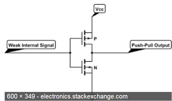
- cmos push_pull.JPG (22.99 KiB) Viewed 362 times
Is the card the one that uses Open Drain in CMD?
If so, that could be a problem.
I haven’t checked if the code disabled the D3 internal pull up, but it can be done if not done yet.
Plz investigate as my know-how from this area is limited.
https://www.design-reuse.com/articles/3 … -core.html 4.1.:
During the Card Identification Mode all the communication is performed via the CMD line and up to 400kHz clock..
PS: ..it is required the sdcard signals (all) have got pull-ups in order to prevent “bus floating” when no sdcard is inserted..
[Pito – Thu Mar 01, 2018 8:12 pm] –
Afaik, the SDIO starts with some low speed clock sequence (400kHz) where it works in SPI mode (and you need pullup at the CMD line) and then it switches to high speed where you do not need any pullup.
Plz investigate as my know-how from this area is limited.
If you mean the card starts in SPI mode then this is not quite correct. The card will start in parallel bus mode but will interpret the signals on DI looking for a specific initial sequence that instructs the card to put itself into SPI mode. When initially powered up (and therefore in parallel mode) the DO from the card is open drain. This is why it requires a pull up. As soon as it is put into SPI mode the pull-up on DO (MISO) is no longer needed. The standard requires an SPI clock speed for putting the card into SPI mode is <= 400KHz before switching to the desired high SPI bit rate.
I have tested lots of cards, hardware implementations, and multiple processor families, over the last 10 years and I have not found a genuine card that I could not initialize at 10MHz. Despite this, I still perform the initialization at 400KHz where possible.
PS: Not to encourage people to remove the SDIO pullups: ..it is required the sdcard signals have got pull-ups in order to prevent “bus floating” when no sdcard is inserted..
The CMD pullup – I would go with 10k max, to ensure fast edges.
A good reading for SDIO interfacing purists: http://datasheet.octopart.com/IP4052CX2 … 555750.pdf
![]()
[Pito – Thu Mar 01, 2018 8:12 pm] –
Afaik, the SDIO starts with some low speed clock sequence (400kHz) where it works in SPI mode (and you need pullup at the CMD line) and then it switches to high speed where you do not need any pullup.
Plz investigate as my know-how from this area is limited.
https://www.design-reuse.com/articles/3 … -core.html 4.1.:
During the Card Identification Mode all the communication is performed via the CMD line and up to 400kHz clock..PS: ..it is required the sdcard signals (all) have got pull-ups in order to prevent “bus floating” when no sdcard is inserted..
It starts at 400Khz, but all lines in PP. According to the other document Squonk shared, the lines d1 to D3 should stay in input mode until the card is switched to 4bit mode, but that’s not what the code does, so I’ll change that. But anyway the errors happen much before.
Identification, changing speed, etc all goes fine. When it comes to transferring data, that’s when the problems start. Specially in read commands.
[Pito – Fri Mar 02, 2018 1:45 am] –
What about the gpios speed setting?
Sorry just saw your post. GPIO was set to 50Mhz.
At the moment I’m leaving the SDIO testing, we know the lines are all traced, SD works to some degree in F1 without pull up resistors, and will test again when I assemble and F4 or F7 board.
The other day I reflowed the MCU to 2nd board I had with all the components for F1 (0R resistors in place of the vcap1 and vcap2), and I can connect to it with st-link with some trouble, but it seems like it’s not running properly. I loaded the bootloader, but the led never blinks, the DFU is not detected in windows, and st-link shows the cpu enters some loop soon. I think it may have to do with the oscillators. I need to compile a bootloader or something else with HSI clock and test again. The crystal seems to be soldered right, and the xtal capacitors too, with no shorts, but I remember in one of the two boards I ended up touching the crystal with the soldering iron, may have been this one, and may have overheated the xtal (iron set to 560F).
When I get a chance to test something compiled for HSI I’ll see if it’s just that or something else. I have checked for shorts between pins, and checked that boot0 and reset get the right levels, and it seems to be right. The MCU does start running code, but then seems to enter a loop, so could be waiting for the PLL to get ready and it never does if the xtal is damaged.
EDIT:
Good and bad news. The good news is that my second board works fine. It was just the led that was not blinking. Not sure why initially the computer were I tried it would not detect the dfu device. May have been some bad solder that I solder later on but thought it was still not working because of the led.
The bad news, is that the sdcard has the same issue as with the first board.
I added ACMD42 to disconnect the D3 internal pull up (doesn’t exist in greyman’s sdfat) took me a while to fine the parameters for the command, but is here in case anyone needs:
http://users.ece.utexas.edu/~valvano/EE … r_Spec.pdf
It didn’t seem to make much of a difference though. It seems that we really need the pull ups with F1. Whenever I have time I plan to reflow an F722 and a F405, that will be more exciting ![]()
Class 2, 2GB, 12Mhz, 4bit wide:
Buffer size 512 bytes
Starting write test, please wait.
write speed and latency
speed,max,min,avg
KB/Sec,usec,usec,usec
3353.24,63927,110,149
3315.44,64452,110,151
Starting read test, please wait.
read speed and latency
speed,max,min,avg
KB/Sec,usec,usec,usec
2110.46,1500545,80,241
5740.16,2335,80,87
5740.16,2335,80,87
5740.16,2335,80,87
Not bad for a 512byte buffer and 12Mhz ![]()
For comparison, the max speed at 12Mhz with 4bit wide is 5859KB, so taking into account the overhead of the code running between transfers, and the time used in sending commands to the card, reading status, etc, the read is pretty much at max bus speed.
[victor_pv – Fri Mar 09, 2018 4:34 am] –
And after a few more changes to the SDIO library (for multiblock read and writes), I get these speeds.
Class 2, 2GB, 12Mhz, 4bit wide:
Buffer size 512 bytes
Starting write test, please wait.write speed and latency
speed,max,min,avg
KB/Sec,usec,usec,usec
3353.24,63927,110,149
3315.44,64452,110,151Starting read test, please wait.
read speed and latency
speed,max,min,avg
KB/Sec,usec,usec,usec
2110.46,1500545,80,241
5740.16,2335,80,87
5740.16,2335,80,87
5740.16,2335,80,87Not bad for a 512byte buffer and 12Mhz
For comparison, the max speed at 12Mhz with 4bit wide is 5859KB, so taking into account the overhead of the code running between transfers, and the time used in sending commands to the card, reading status, etc, the read is pretty much at max bus speed.
Haven’t been following the discussion that closely. But if i understand correctly, the issue is that on the F103 you can’t enable the pullups when the pins are in SDIO mode? that would indeed give issues and require external resistors for f103 boards.
I have had little time (and will have little time the coming weekends) to continue testing with my board :s. but i’m eagerly following this thread, and happy with where we already are ![]()
[racemaniac – Fri Mar 09, 2018 4:03 pm] –
…if i understand correctly, the issue is that on the F103 you can’t enable the pullups when the pins are in SDIO mode? that would indeed give issues and require external resistors for f103 boards.
Correct, alternate mode in F1 is always push-pull, unlike the F3 or F4 where you can enable pull up or down at the same time. And my tests with different boards and sdcards seem to confirm we need the resistors for high speed.
Still can achieve a respectable speed by using the 4bit wide mode at slower speeds, so the sd is not totally unuseable.
I am thinking on adding speed fallback to the F1 SDIO library, so in case of errors if reduces speed before failing.
Currently i have implemented a retry mechanism for writes if the card report a CRC error. Shouldn’t be much more effort to add code to reduce the speed to a safe 2-4Mhz before retrying.
Does that make sense?
The pullups are required for a) avoidance of floating when the card is not in, b) during init at the CMD pin as it is used in OD mode (afaik).
There is something else causing the issue. The tracks are short, so excessive ringing is not the case perhaps.
Crosstalk? Vcc decoupling? The capacitor at Vcc (close to the card socket) shall be at least 10-22u ceramic multilayer.
Also, with F1 it could be a crappy silicon – using sdio with F1 is rare.. May be it does not work properly per se.
PS: PP may require “impedance termination” with longer cables. For example imagine an 1meter long flat cable. Driven by PPs (~150ohm impedance). At the other end there will be say 330ohm against GND and 330ohm against Vcc wired at each line (that means ~150ohm termination which match the PP impedance at the other side, the flat cable wires pairs are also ~100-150ohm impedance). But your board is not that case.
[Pito – Fri Mar 09, 2018 10:55 pm] –
The PPs do not need pullups. PPs are “low impedance” – maybe 100-200ohm, thus any pullup >1k makes no sense.
The pullups are required for a) avoidance of floating when the card is not in, b) during init at the CMD pin as it is used in OD mode (afaik).
There is something else causing the issue. The tracks are short, so excessive ringing is not the case perhaps.
Crosstalk? Vcc decoupling? The capacitor at Vcc (close to the card socket) shall be at least 10-22u ceramic multilayer.
Also, with F1 it could be a crappy silicon – using sdio with F1 is rare.. May be it does not work properly per se.PS: PP may require “impedance termination” with longer cables. For example imagine an 1meter long flat cable. Driven by PPs (~150ohm impedance). At the other end there will be say 330ohm against GND and 330ohm against Vcc wired at each line (that means ~150ohm termination which match the PP impedance at the other side, the flat cable wires pairs are also ~100-150ohm impedance). But your board is not that case.
The card and the host transition from out to in and back to out depending who needs to send the data. In between those transitions, the lines are floating with neither end pulling it up or down, so the end that is expecting data and reading may get spurious signals and mess the incoming data so it fails CRC.
For example when the host sends a command to the card to read a block, the card is in input mode, the host sends the command and switches to input mode, the card then switches to output to send the block, but before the card switched the host may have switches already and is reading on a floating line.
There is a good article about all that, with actual oscilloscope captures, making the point for pull ups. If I can find it I’ll post it. I don’t see an easy way to solder resistors without a big mess up, if I do, I will definitely test it. I may test a 1 bit mode with an external sd module, and test if adding pull ups makes a difference.
About capacitor, I have tested with 2 different 10uF capacitors, both MLCC, one in 0805 size, and one is 0603 size, and in line with VCC there is an inductor, I have tested with the inductor in one board, and with a ferrite in the other board. Similar results in both cases.
Ideally, what I need is an analog oscilloscope and we wouldn’t have to speculate, but I don’t have one.
If I remember right the CMD in is OD only in SDI/O mode, not for memory SDCard. For memory cards is always PP.
Would be great to see the paper on the issue, sure..
I’m sure that the cards driver strength has something to do with it, since at some speeds I don’t get write errors (that’s when the card actually pulls the most current, and a problem with VCC may cause the most effect), and the card is verifying the CRC, and reporting it back as valid, but I get read errors, when the card is driving the lines, and the host is reading.
I believe there is some driver strength setting for the cards, but haven’t looked at that yet.
If you have a good oscilloscope and time to look at this, I can ship you one of this cards.
CMD6 sets the sdcard into High Speed Mode (>=50MHz). That is the only switch with 3.3V signalling. The default mode is 25MHz.
Most settings there are with 1.8V signalling only (we do not use).
- CMD6.JPG (85.48 KiB) Viewed 683 times
Thus SDR12 => ~6MBytes, SDR25 => ~12MBytes, SDR50 => ~25MBytes, SDR104 => ~52MBytes and DDR50 => 50MBytes ?
So, make sure to use SDR25 mode for a class 10 card to get full speed access.
With the F1 I haven’t been able to get reliable transfers with a clock faster than 12Mhz. F1 in theory it could go up to 48Mhz, but I haven’t been able to test.
Pito, thanks for checking, I knew there were some settings but had not looked at the details yet.
At the moment I only implemented the part to disable the D3 pullup, which did not make a difference, but since we don’t use 1.8V, we can’t test the rest. If it fails at high speed with 3v3, I suspect with 1.8V could be even worse no matter the settings.
EDIT:
I did more changes to the library so Steve’s bench test would work fine, then I commented out the section of code where it tries to see if the card supports high speed mode and set it (SDR50, using CMD6), so it will not try to do that now and just leave the card in the default speed mode. With that I can get the 16G card working in 4bit mode up to 12Mhz (previously 4Mhz seemed the top reliable speed).
When I get errors during write, often times is this flag:
#define SDIO_STA_STBITERR (1<<9) // Start bit not detected on all data signals in wide bus mod
Test results, 16GB class10, 4bit wide 12Mhz:
######################################################

Demo sketch of STM32F4 SDIO (DMA) implementation.

######################################################
init time: 0 ms
Card type: SDHC
Manufacturer ID: 28
OEM ID: BE
Product: SDU16
Version: 1.0
Serial number: 2f000000
Manufacturing date: 4/2012
cardSize: 16012.80 MB (MB = 1,000,000 bytes)
flashEraseSize: 128 blocks
eraseSingleBlock: true
OCR: c0ff8000
Volume is FAT32
blocksPerCluster: 64
clusterCount: 488416
freeClusters: 488413
freeSpace: 16004.32 MB (MB = 1,000,000 bytes)
fatStartBlock: 8752
fatCount: 2
blocksPerFat: 3816
rootDirStart: 2
dataStartBlock: 16384
FreeStack: 55503
######################################################
Type any character to start
>>Send to COM3: "1"<<
Test started - please wait, it may take up to 3 minutes
size, write, read
bytes, KB/sec, KB/sec
512, 4507.83, 5131.75
1024, 5066.29, 5511.97
2048, 5351.16, 5658.31
4096, 5484.59, 5736.69
totalMicros 1589389
yieldMicros 1434590
yieldCalls 7696
yieldMaxUsec 2944
kHzSdClk 12000
Done
I’ll try to make some time monday to get my F4 board up & running
The SDIO works fairly well after my last batch of modifications without the pull up resistors, it just can’t get to the full speed that it could otherwise, but still plenty of speed with little cpu utilization.
I am hoping to have time to assemble an F405 and an F722 this weekend, we will see…
Did anyone else have any problem with the RGB leds from ali?
I ordered some more from mouser, but ended up sending all of them to Michael, so I don’t have any from mouser to test.
I ordered this:
https://www.aliexpress.com/item/100pcs- … 0.0.lXlNLK
They don’t show any information about what pin is the common anode, but it is the same pin as in this link:
https://www.aliexpress.com/item/100pcs- … 20763.html
But in the bluepillF4 pcb I can see the common pin is top left, not top right.
Can someone confirm that I am not doing something wrong?
I ordered the same part from the same supplier and it worked fine for me. So I suggest you double check your issue.
The common anode is marked with a green dot on the reverse side and, as you can see from the photo, is the pad where the three anodes are connected.
- rgb.jpg (53.16 KiB) Viewed 376 times
the HSI and HSE clocks worked well (after resolving a CubeMX issue).
i’m always curious, so what issue, how does it show up and the cure ?
stephen
I have 2 boards ready to mount the MCUs, not sure if I’ll go thru the trouble of trying to remove the leds to place RGB ones, may give it a shot.
I am planning to mount an F405 and an F722 in these two.
I haven’t made any progress anymore with my board, i’ll try to make a second one in the near future to test with, using the knowledge we gained since my first attempt (and i hope with better soldering than my first attempt :p )
So far I have reflowed 4, first two with low temp solder (SnBi), only had 1 component that move either during solder or when placing the boards in the oven.
Then the last two with SnPbAg solder, and 1 of the 22ohm resistors in one of the boards moved, and need to correct that with the iron.
With the low temp solder is fairly easy to remove/replace a component since it melts really easy. A bit more trouble with the normal temp one. But in both cases everything reflowed fine and the switches survived the reflow profiles without any trouble.
I bought one of these silicone pads:
https://www.aliexpress.com/item/S-170-S … 81619.html
it has little numbered squares in one side (#6 in the photos), so I first place all my components in those spaces, following the numbers as per the component list, then apply solder to the boards with laser cut stencil, and place the each component in both boards at the same time. I think it takes me much longer to pick each component and place the required quantity in the mat, than to apply the solder, place the components in the boards, and reflow them. Having them all sorted in the mat helps a lot.
- F722.jpg (50.05 KiB) Viewed 396 times
[zmemw16 – Tue Apr 03, 2018 9:11 am] –
@eggsylah wrote
the HSI and HSE clocks worked well (after resolving a CubeMX issue).i’m always curious, so what issue, how does it show up and the cure ?
Well it was probably my fault in mis-configuring the Clock Configuration and I can’t reproduce it now.
But essentially the following loop never terminated
  LL_RCC_SetSysClkSource(LL_RCC_SYS_CLKSOURCE_PLL);

/* Wait till System clock is ready */

while(LL_RCC_GetSysClkSource() != LL_RCC_SYS_CLKSOURCE_STATUS_PLL)

{

}
[victor_pv – Wed Apr 04, 2018 3:36 am] –
I am the proud owner of the first and only (so far) BluepillF7 board!!
Very Nice!!
Previously, you inspired me to order the F7 chips too so I will have to try that later. I think I should do an F405 or F411 first though.
Eric
[victor_pv – Wed Apr 04, 2018 3:36 am] –
I am the proud owner of the first and only (so far) BluepillF7 board!!
F722.jpg
woow, nice XD
I think the L476 may be one of the best options for this board, taking in account we have low quiescent current regulators and a battery charger.
The F722 is more of an experiment, since several pins are are in a different position, and we lose access to PB0 and PC5 if I remember right, but if it works fine, then we could design a specific version with corrections for the F7.
I still need to add vcap1 (surprised the core works at all without it), and then flash some blinking sketch.
I noticed the blue led blinks, I didn’t check the schematic but I imagine the pin is shard with one of the SWD pins. Did you guys see the same? the blue in the rgb led blicking when connected to stlink?
With a BMP connected I’m blinded by the green LED — enough for it to be a distraction. I’ll have to look if it’s really necessary for the BMP to pull that down so strongly.
Also the power LED D1 was too bright so I removed that from the board.
Finally, I noticed in the F103, F405 and L462 datasheets there is always something like (just search for PC13):
Due to the fact that the analog switch can transfer only a limited amount of current (3 mA),
the use of GPIO PC13 to PC15 in output mode is restricted: the speed has to be limited to
2 MHz with a maximum load of 30 pF and these I/Os must not be used as a current source
(e.g. to drive a LED).
I believe that is a total of 3mA not 3mA each – so should we really be using PC13 to drive the red LED?
It seems to work fine on my board and the bluepills all do it but perhaps some other GPIO would be better.
I see this was briefly mentioned before in viewtopic.php?t=117&start=130
Thanks for the offer of more boards. I’ve only used 1 so far so it isn’t necessary yet.
I’ve mounted the 6280 now so everything but the LiPO and SD components are installed. I won’t add these to this board so now I need to try some USB and OTG sutff – this will be a bit of a learning curve.
Oh and check the LSE oscillator / RTC.
Eric
With today’s LEDs you do not need much current.. 3mA is a _lot_ of current..
Most LEDs lit fine with 0.5mA or less (provided you want the LED to be used for indication purposes only)..
R_led = (3.3V – Vf_led)/0.0005A
Vf_led: red 1.6V, green/orange 2V, blue 2.5V
Best you try with your LED and a resistor before you solder the stuff in (3.3V – LED – R – gnd).
In my first 2 boards (F1), I didn’t use RGB led, but a red led for power and another one for user led.
In both I used 1K resistors. I estimated about 1.5mA if the leds drop 1.8V. I forgot if I measured the voltage drop, or I tested with a 1K resistors before assembling, but at that point I decided that was enough for the red leds.
In the next 2 boards (405 and 722), I used green led for power. Since the green led is so much brighter, but has a higher voltage drop, I wasn’t too sure, but decided to also use 1K resistors, and they are still way too bright.
I measured voltage drop after assembly, and was 2.7-2.8V if I remember right, so about 0.5mA with a 1K resistors, and still very bright.
At first I did not assemble the RGB, until Eric pointed out I could use them sideways, so at that point I removed the user led (also green in this case) and assembled the RGB. Since both the red and green were bright enough with double the resistor value, I did the same for the blue led and used a 510ohms resistor or something like it.
I haven’t tested the RGB other than seeing the blue blink with the SWD signals, not very bright though.
One of my concerns was that we took care of using a low quiescent regulator, so wouldn’t make sense to have a led drain a lot of power, so I wanted to try powering the leds with the minimum current that would still be usable. I’m almost sure I could still double the values again in the resistors and the leds would still be bright enough to be used indoors, may be not so much in a bright day outside.
Now, all my leds are from Ali, so I really have no clue how close they really are to the specs the seller published.
Repeating this with reputable leds would like be the best, but going forward I plan to use the doubled values as standard, and only adjust up or down if I after assembly they are not bright enough, and for low power, I think keeping a green used led with a 2k resistor is still probably bright enough.
I didn’t post about using double the resistors because I really can’t point to real specs for the leds I am using, so would be risky to advice others to change the values.
Now based on my results and Eric’s results with the green led, I would say he is safe to use at least 1k-1k5 resistors for red and green, and likely 500 or so for blue.
@Pito, I often see higher voltages for Green at equal current, more similar to blue leds, although for all of them the voltage changes exponentially with the current, so it’s hard to say a voltage drop for sure without knowing the supplied current, and who is the vendor. Also since the green tends to be brighter, it seems to make sense to keep the current lower to get similar brightness across the three.
As example, this wurth RGB shows over 3V at 5mA for green and blue:
https://www.mouser.com/datasheet/2/445/ … 113677.pdf
But this from liteon shows about 2.8V for the same current:
https://www.mouser.com/datasheet/2/239/ … 141816.pdf
Using the same resistor for both would result in very different currents.
With aliexpress leds I agree with you the best is to get your led and test.
Also because the LEDs are being produced by thousands vendors who gathered the know how via their in-house R&D depts ![]() , the V-I characteristic might be pretty different.
, the V-I characteristic might be pretty different.
In past I purchased about 20 smd diodes of all available colors and provenience they had on stock and did a measurement – I set the luminosity (by changing the R) such all the LEDs lit “the same intensity” visually, and, they were visible during the daylight inside a room blinking (indication purpose). The currents were minuscule.. I can remember some lit fine with 10k resistor. Mostly around 3k9+.
There is a “not good engineering practice” in that regard coming from early eighties (40y back) – where the datasheets of all LEDs at that time listed “If=20mA” and the LEDs at that time indeed needed 20mA to lit visibly.
Most datasheets do it till today ![]() And based on that “20mA” information many designers of our lovely boards are still using R=200-500ohm.. Some advantageous ones go even 1k
And based on that “20mA” information many designers of our lovely boards are still using R=200-500ohm.. Some advantageous ones go even 1k ![]()
So to know how many mA you are feeding the led, you have to measure the voltage drop across the led, that gives you the voltage drop in the resistor, and from that you can calculate the I. Just knowing the resistors value is not enough. Specially since the voltage drop varies greatly with the current. So changing a 1K resistor for a 2K one doesn’t necessarily result in half the current.
That’s why I measured voltage drop, I knew R, since I decided it, and knew VCC, since it’s always the same. Without knowing the voltage drop, R doesn’t tell me anything about the current in the led. As you know the same 1k resistor in a red led dropping 1.8V will result in a different current than if the led was dropping 2.8V. So 2 leds from 2 different vendors may produce the same exact lumens with the same current, but if the voltage drop is different, driving them with the same serial resistor results in a different current.
That’s why I didn’t post about my resistors values. Someone else may have a red led that drops move voltage and a green that drops less, and my values wouldn’t give the same result.
in the case of the green led, I measured about 2.8V, with the 1K resistor that was about 0.5 mA. The red led if remember right was dropping 1.8V with the same 1K R, so was getting about 1.5mA. The green is still a bit brighter, but not a whole lot.
Since the blue led voltage drop is supposed to the green one, but produces less lumens with the same current, I used a 500ohm R, but have not measure the drop in that one, so no idea yet how much current goes thru it. I would expect around 1mA.
A diode may have a voltage drop of 0.698V with 1mA, 0.703V with 10mA, 0.706V with 100mA, 0.711V with 1A.
That is the exponential nature of V-I..
Use ammeter instead (in series with R). That is how the current driven devices are managed.
The transistor is the same – you do not measure the Vbe=0.7V drop but you set Ib via an Rb.
PS: You may see the huge change of If current at small change of voltage drop (Vf)
from https://electronics.stackexchange.com/q … th-voltage
- LED V_I char.JPG (39.52 KiB) Viewed 734 times
I do not need an amp meter in series when I know the resistor and the voltage, I = V/R, and V in the resistor is V=Vcc-Vdrop.
So for a given VCC, which I know, and a given R which I know, I only need to know the V drop across the led to know the current in the resistor, which is the same across the led since the are in series.
We both know the voltage drop is not the same across the range or currents, and not even the same for the same current across manufacturers. That’s what I have been saying from the start, that I didn’t post my resistor values initally because with my leds being from Ali, I can’t say which other leds are going to have the same voltage curves.
I only posted them to let Eric know what worked for my leds, and how much current mine are getting and still are bright, so he can try to match similarly with his leds.
Right, when you know the resistor’s value and the voltage drop across the resistor (or across the diode) you may know the current well.
viewtopic.php?f=3&t=4058&start=20#p48757
Moreover, the new STM32F7 “Value Line” CPUs from ST (discussed in yet another thread here) may render the BluePill F4 board even more atractive, as these CPUs are both cheap, powerful and available in an LQFP64 package (STM32F730R8) almost compatible with the ones used for the BluPill F4 board as it is today.
I will try to summarize the outstanding issues below:
- Voltage Sense: Use 1% tolerance for the resistor bridge. 2x 10 kohms should be OK, since the absolute maximum voltage given by the AP2114HA (U1) and AP2112K3.3 (U2) is 6.5V, while their recommended maximum value is 6.0V, whereas the ADC on PC1 is having a 3.3V maximum input voltage. This resistor bridge is permanent and will consume a nominal 250µA @5V +VIN. If power consumption is critical and input voltage sense is not required, one can remove R21.
- LEDs: the power LED D1, as well as the single red LED on PC13 or the RGB LED on PC13/PA13/PA14 all seem to work fine, although their limiting resistors need to be adjusted to reduce current and brightness to a reasonable value. And yes, the red LED is on PC13 which is not meant to drive LEDs, but it is on purpose for compatibility with the original BluePill. And yes too, the green and blue LEDs are shared with the SWD, causing psychedelic effects while flashing the device over JTAG If the RGB LED isn’t required, it can be replaced by a single red LED on PC13, as the footprint is compatible between the 1616RGB and 0603 LED.
- User button: the 0R R5 series resistor should be replaced by a higher value (apparently up to 2k is OK) to avoid shorting PB8 when the button is pressed. EDIT: I need to remove the GND TAB from the footprint to avoid shorts
- Reset button: the reset button is wrong: it should short to ground when pushed. This can be fixed by removing R6 and soldering one of its pad to GND, but this need to be fixed in the next revision of the PCB. EDIT: I need to remove too the GND TAB from the footprint to avoid shorts
- SWD: It seems to work fine, a test with R20 removed and LiPo charger installed still needs to be performed to validate powering the board while flashing from the +VIN or battery instead of the supplied +3.3V from JTAG. Note that using the LiPo charger will be incompatible with the standard BluePill in this regard.
- SDCard: This is the most controversial part. First, the connector used allows removing the SDCard with the USB cable plugged, but it was originally a much lower profile connector with the SDCard pointing towards the center of the board “under the belly”. Then there seems to be a big mess with the required/not required pullups on the signals: they seem required for STM32F1, but not for STM32F4/F7. There were some speed tests using the different CPUs, but I don’t know if they can be considered OK or not. Also, the hot-plug behavior needs to be tested to see if decoupling is good enough or if this will trigger a CPU reboot. As for the pull-up resistors, I will check it it is possible to add them to the layout without too much hassle.
- USB: USB devices seems to be working fine, but the USB host and its current/voltage protection and control need to be tested completely.
- Crystals:There have been some testing with both the 32kHz and 8MHz crystals, but I am not sure of what is working or not, and what are the values for the stray capacitors. There was a swap between their values in my first design.
- CPU: At least the STM32F103, STM32F405 and STM32F722 were tested successfully, although the latter would require a modification to put the VCAP_1 capacitor on the right pin that is moved one position left compared to the other packages (this will also be the case for the new STM32F7 value line CPUs). I will see if I can provide a footprint to mount it as an option on the PCB.
- LiPo Charger and Ideal Diode: This is totally untested. Although it is the same circuit as the one used by Olimex in its ATMega32U4 board, this needs to be fully tested.
- Digital Power: It is working, but we need to perform some load test to check how much current it can handle and if there is a temperature issue.
- Analog Power: This needs to be tested, and in particular what is the noise floor level, in order to determine if a 4-layer board is required to get fully separate digital and analog grounds.
What I am not sure is what sotware tools should be used to test these basic features: as most are really low-level (like crystals), the Arduino cores are not the best guess. Please let me know your setups, if possible using free tools.
That’s some hard issues that are left to test ^^’
Any ideas how you’d want to stress test the “digital” power rail?
Also, from the conversation in another topic I got the impression that the design will need to be based on a 4-layers PCB. Is it not the case, and we may walk away with just 2 layers? (just trying to understand what we base our costs estimations on)
[andrewju – Tue Sep 04, 2018 7:48 pm] –
I didn’t read the whole thread yet, so please excuse me if I ask something that was already discussed. I see the compatibility with F1 chips requires some hardware modifications (that are currently there). Is F1 support needed at all, or should we just keep this design as an F4 / F7 only, for simplicity?Also, from the conversation in another topic I got the impression that the design will need to be based on a 4-layers PCB. Is it not the case, and we may walk away with just 2 layers? (just trying to understand what we base our costs estimations on)
Dropping F1 compatibility is indeed an option we can discuss (i think we kept going for it since our main core (libmaple) is best at supporting F1.
And regarding the 2 layer: 2 layers may be enough, but it’s likely that 4 layers will be superior. We’ll have to do noise measurements on the analog part, and there is probably a good reason why all decent boards with little analog noise are 4 layers ^^’. but to be investigated with our current prototypes.
If anyone has suggestions on how to measure the analog noise, i have the equipment, but it’s not something i’ve done before ^^’.
[andrewju – Tue Sep 04, 2018 7:48 pm] –
I didn’t read the whole thread yet, so please excuse me if I ask something that was already discussed. I see the compatibility with F1 chips requires some hardware modifications (that are currently there). Is F1 support needed at all, or should we just keep this design as an F4 / F7 only, for simplicity?Also, from the conversation in another topic I got the impression that the design will need to be based on a 4-layers PCB. Is it not the case, and we may walk away with just 2 layers? (just trying to understand what we base our costs estimations on)
F1 support is only affecting the BOM: the first mod is R6 1.5k USB pull-up which is required for F1, whereas it should not be mounted for F4/F7, as it is USB OTG with built-in pull-ups. The second mod is regarding the VCAP_1 and VCAP_2 2u2 capacitors required fior F4/F7, that need to be replaced by 0R for F1, where these pins should be connected to GND.
As you can see, only 3 small changes in the BOM between F1 and F4/F7, with nearly no impact on the cost.
Regarding the 2-layer vs. 4-layer, it will depend on the noise measurement on the analog part: having a 4-layer design will help to get separate analog and digital GND.
For the measurement methods, @Pito will probably have a very good idea on how to measure this noise!
[racemaniac – Tue Sep 04, 2018 8:20 pm] – If anyone has suggestions on how to measure the analog noise, i have the equipment, but it’s not something i’ve done before ^^’.
You will have to get the digital values out of the ADC and do an FFT to turn them into the spectral domain for analysis. Measuring the peak and noise floor in the frequency domain will give you the SNR (Signal to Noise Ratio), that you can compare between using the analog LDO and the simple ferrite bead and see if this makes a difference or not (it shouldn’t IMHO).
But this is not enough to see how much the power supply affects the ADC performance.
Here is a very good article on the subject:
http://www.analog.com/en/technical-arti … d-adc.html
Please note that there is a small error in this article: one should read “11.26 nV rms/sqrt(Hz)”, rather than “11.26 nV rms”.
This article explains how to measure the PSRR-dc (Power Supply Rejection Ratio in dc), the PSRR-ac (Power Supply Rejection Ratio in ac) and the PSMR (Power Supply Modulation Ratio) for a given ADC.
The PSRR-dc (how the ADC may change with a change in power supply voltage) is not very useful, but the PSRR-ac (adding an ac signal on top of the dc power supply) is much more interesting. Note that it depends on both power supply voltage and frequency, so you will have to sweep over both values, with the ADC input signal grounded and a filter to mix the perturbing signal with the power supply:
PSMR tells how sensitive the ADC is to power noise effects as it modulates with analog input signal applied:
Then along with the ADC SNR, ADC resolution, p-p full scale input range and sampling rate, you will be able to compute the ADC quantification noise in Vrms and its noise density in Vrms/sqrt(Hz), that you can compare with the regulator’s one over the frequency band of interest, attenuated by this PSRR-ac value and see if it degrades the ADC performance or not.
I don’t have the test equipment (2x lab power supplies, 2x signal generators, 1x scope and MatLab to do the FFT), so if you have all these, good luck!
[madias – Wed Sep 12, 2018 10:33 pm] –
(Addition) Maybe I’m wrong, but measuring the noise floor should be done with USB disconnected and battery powered avoiding “false positives” caused by a bad/average USB hub (internal or external) or power supply (unless it’s a “real” LAB one).
+1
[madias – Wed Sep 12, 2018 10:33 pm] –
(Addition) Maybe I’m wrong, but measuring the noise floor should be done with USB disconnected and battery powered avoiding “false positives” caused by a bad/average USB hub (internal or external) or power supply (unless it’s a “real” LAB one).
Absolutely!
The paper’uses lab (bench)’power supplies. If you use the power supply from USB, you are not performing SNR/PSRR/PSMR measurements but common-mode EMC tests!
Do i just connect battery, measure SNR, and that’s it.
Or do i connect battery, connect an i2c, spi & sd card & some leds, so i really make some noise on the digital side, and then try?
Then once you are sure that the power supply is good, you can try to add noise sources to see if there is a problem with the ground paths and where.
[racemaniac – Thu Sep 13, 2018 5:43 am] –
And are there specific situations that would need to be measured?
Do i just connect battery, measure SNR, and that’s it.
Or do i connect battery, connect an i2c, spi & sd card & some leds, so i really make some noise on the digital side, and then try?
Hm. I think the first premise is to check the board layout not external peripheries. So the external peripheries should make as less noise as possible. It’s all about the indifferences between the data/sck lines of the peripheries and the ADC channels.
Maybe it would help to examine the blue pill layout as a negative example and what causes the noise on the ADC channels. I think 4 layers are a good thing, but there are 2 layer boards long time before without such issues. Ok, the small board size is not your friend for this task ![]()
[Squonk42 – Thu Sep 20, 2018 7:31 pm] –[racemaniac – Thu Sep 20, 2018 7:15 pm] – I’ve been working a bit on this the past week, hope to have some results by saturdayThank you!
I checked the original NUCLEO-F103RB from ST, it is a 2-layer PCB (checked the gerbers) and they use a simple 0603 600 ohms 500 mA ferrite bead (Taitec FCM1608KF-601T05, checked the BOM) and ordered this board to compare it to both an original Bluepill and to our Bluepill F4.
Working on it atm, and wondering: i have a lot of stuff, but not a signal generator >_<. Would generating the noise from a PWM pin be sufficient to do this testing (this is what i’m currently giving a try), or do we need someone more equipped to perform this really properly >_<. I’ve got a decent scope, but a signal generator is not part of it ^^’
https://www.instructables.com/id/Square … 5-Timer-1/
or just a transistor + cap(s):
https://blog.jongallant.com/2015/01/sim … nking-led/
Build a battery powered circuit to prevent noise.
[madias – Sat Sep 22, 2018 5:52 pm] –
Do you have one of those 555 timers?
https://www.instructables.com/id/Square … 5-Timer-1/
or just a transistor + cap(s):
https://blog.jongallant.com/2015/01/sim … nking-led/
Build a battery powered circuit to prevent noise.
I think i have some 555’s laying around. in which way are they better than just pwm’ing a pin?
What should be exactly the task for the “signal generator”?
[madias – Sat Sep 22, 2018 8:15 pm] –
Depends on your needs:
What should be exactly the task for the “signal generator”?
Look at the article Squonk quoted, there they use a signal generator to insert noise of specific frequences into the power supply, and then measure the response of the ADC to that noise
http://stm32duino.com/viewtopic.php?f=1 … 840#p49264
Basically, you need to generate a pure sine wave that may be either full-swing peak-to-peak or -20 dB of it (e.g. 1/10th).
First, you inject it full-swing to the ADC input with a clean power supply to determine the SNR by looking at the ADC output in the frequencies domain. The theoretical SNR depends only on the ADC resolution in bits (74 dB for 12 bits), but the real one will be much lower depending on routing, ground path, noise on the power supply, etc. This is good to know, but it won’t tell you how much you will be able to gain by changing the power supply, routing, etc. To do this, it is necessary to measure ho much the ADC is affected by the power supply, what is left will be due to the bad/good signal routing and ground quality.
This is why the next step is to ground the ADC input and first varies the power supply voltage to see how much it affects the ADC in DC mode (PSRR-dc), no need for a generator to measure the DC offset error, but you will need it full-swing applied to the ADC input in order to measure the gain error.
Then, you inject the generator -20 dB output into the analog power supply using a notch filter to see how much it affects the ADC (PSRR-ac). This varies of course with the generated signal frequency, and since you need to use a filter to mix the perturbing generator with the power supply, you will need to adjust the power supply level to compensate for the filter and/or change the filter with the measured frequency bands.
Then last, you will need 2 generators (one for feeding the ADC input full-swing, the other to inject perturbations @ -20 dB into the ADC power supply) to see how much the perturbing signal modulates the ADC input (PSMR).
As explained before, along with the ADC SNR, ADC resolution, p-p full scale input range and sampling rate, you will be able to compute the ADC quantification noise in Vrms and its noise density in Vrms/sqrt(Hz), that you can compare with the regulator’s one over the frequency band of interest, attenuated by this PSRR-ac value and see if it degrades the ADC performance or not.
- a reference board (I was thinking of the low-cost NUCLEO-F103RB) featuring the STM32F103RB and a ferrite bead-based analog power supply
- the original Bluepill with no separate analog power supply (bad, bad, bad…)
- our Bluepill F4 with the separate analog LDO
- our Bluepill F4 with the simple ferrite bead
… and compare them to see what we get.
We should then be able to see how the Bluepill F4 performs against the other ones, and if the analog LDO makes a significant difference or not.
But it won’t tell us how much we would need to improve the power supply to get the best ADC performance, and if the problem would be solved by using a 4-layer board or not.
[Squonk42 – Sat Sep 22, 2018 9:03 pm] –
Yes, check my previous post above:
http://stm32duino.com/viewtopic.php?f=1 … 840#p49264Basically, you need to generate a pure sine wave that may be either full-swing peak-to-peak or -20 dB of it (e.g. 1/10th).
First, you inject it full-swing to the ADC input with a clean power supply to determine the SNR by looking at the ADC output in the frequencies domain. The theoretical SNR depends only on the ADC resolution in bits (74 dB for 12 bits), but the real one will be much lower depending on routing, ground path, noise on the power supply, etc. This is good to know, but it won’t tell you how much you will be able to gain by changing the power supply, routing, etc. To do this, it is necessary to measure ho much the ADC is affected by the power supply, what is left will be due to the bad/good signal routing and ground quality.
This is why the next step is to ground the ADC input and first varies the power supply voltage to see how much it affects the ADC in DC mode (PSRR-dc), no need for a generator to measure the DC offset error, but you will need it full-swing applied to the ADC input in order to measure the gain error.
Then, you inject the generator -20 dB output into the analog power supply using a notch filter to see how much it affects the ADC (PSRR-ac). This varies of course with the generated signal frequency, and since you need to use a filter to mix the perturbing generator with the power supply, you will need to adjust the power supply level to compensate for the filter and/or change the filter with the measured frequency bands.
Then last, you will need 2 generators (one for feeding the ADC input full-swing, the other to inject perturbations @ -20 dB into the ADC power supply) to see how much the perturbing signal modulates the ADC input (PSMR).
As explained before, along with the ADC SNR, ADC resolution, p-p full scale input range and sampling rate, you will be able to compute the ADC quantification noise in Vrms and its noise density in Vrms/sqrt(Hz), that you can compare with the regulator’s one over the frequency band of interest, attenuated by this PSRR-ac value and see if it degrades the ADC performance or not.
what do you mean by “yes” XD
– yes i’d need a signal generator
– yes a 555 would be better
– yes doing it with a pwm pin to start out would be ok
I don’t know how long you want to wait, but on a quick search on ali if found this:
https://www.aliexpress.com/item/Functio … 53613.html
The XR2206 is an excellent signal generator chip and if the guys didn’t f*** up the circuit it’s highly recommended for such a task. (Up to 1 MHZ)
Even the ICL8038 is a good chip: (slightly cheaper, but only 50-5KHz (can be modified))
https://www.aliexpress.com/item/ICL8038 … 43651.html
Battery powered they should give a perfect sine wave.
(For myself I build some VCO’s in the past with both chips)
[madias – Sat Sep 22, 2018 10:18 pm] –
As Squonk42 said you need at least one sine generator (555 is only tri/sqr really not recommended for a “pure” sine wave):
I don’t know how long you want to wait, but on a quick search on ali if found this:
https://www.aliexpress.com/item/Functio … 53613.html
The XR2206 is an excellent signal generator chip and if the guys didn’t f*** up the circuit it’s highly recommended for such a task. (Up to 1 MHZ)
Even the ICL8038 is a perfect chip: (slightly cheaper, but only 50-5KHz (can be modified))
https://www.aliexpress.com/item/ICL8038 … 43651.html
Battery powered they should give a perfect sine wave.
(For myself I build some VCO’s in the past with both chips)
I’m wondering what the record is of being active on this forum without ending up buying something XD
a few weeks?
But you can buy the XR2206 at your local electronic store for nearly nothing an build up your own circuit – it’s an interesting chip
https://www.google.at/search?q=sine+wav … yPsi5bwFKM:
How about “self testing” the board? Both (F405&F411) have 12Bit DAC’s:
So just generating a look up table (or calculate the sine wave on the fly) -> DAC -> into ADC input(s). Sample the input and compare it to the output of the DAC’s (both are 12 bit) . The DAC Output can also physically damped via a Potentiometer if needed. On other pin’s they could some generated PWM outputs (also inserted into different ADC) as a “noise factor”?
[madias – Sat Sep 22, 2018 10:52 pm] –
Maybe a totally dull idea:
How about “self testing” the board? Both (F405&F411) have 12Bit DAC’s:
So just generating a look up table (or calculate the sine wave on the fly) -> DAC -> into ADC input(s). Sample the input and compare it to the output of the DAC’s (both are 12 bit) . The DAC Output can also physically damped via a Potentiometer if needed. On other pin’s they could some generated PWM outputs (also inserted into different ADC) as a “noise factor”?
I’m currently working with a bluepill to at least measure the issue we’re trying to solve XD. And the bluepill doesn’t have a DAC.
[madias – Sat Sep 22, 2018 10:52 pm] – Maybe a totally dull idea:
How about “self testing” the board?
Well, maybe not a good idea in this case, since what we want is to measure the ADC SNR, ground and analog power supply problems ![]()
If doing so, we will mix ADC, DAC, ground and power supply problems and will not be able to measure anything meaningful.
You can use a PWM or DAC from a separate MCU, but this will require a rather good output filter to achieve a good THD < 0.1%.
The XR2206 and ICL8038 are good enough for low-quality audio band, but not much more: their BW is < 100-500 kHz, they have a 1-2% (-34 to -40 dB) THD and they require a > +10V power supply.
I would recommend a cheap AD9833-based DDS module, only $1.94 on Ali:
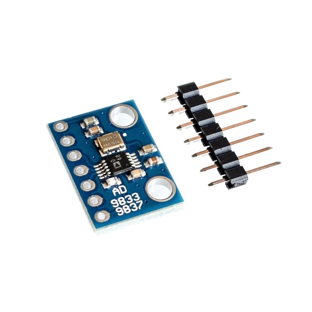
https://www.aliexpress.com/item/sku/32837067609.html
These have a more standard +2.3V to +5.5V power supply, a 12.5 MHz BW, and a typical THD of -66dB (0.05%) : they are good for a 10 MHz AWG (Arbitrary Waveform Generator), and they can be controlled from SPI.
But here, we would rather use one of these < $50 2-Channel 6 MHz BW instruments from Ali or eBay:
https://www.aliexpress.com/item/sku/32822689317.html
https://www.ebay.com/itm/263536180453
[Squonk42 – Sun Sep 23, 2018 8:26 am] –[madias – Sat Sep 22, 2018 10:52 pm] – Maybe a totally dull idea:
How about “self testing” the board?Well, maybe not a good idea in this case, since what we want is to measure the ADC SNR, ground and analog power supply problems
If doing so, we will mix ADC, DAC, ground and power supply problems and will not be able to measure anything meaningful.
You can use a PWM or DAC from a separate MCU, but this will require a rather good output filter to achieve a good THD < 0.1%.
The XR2206 and ICL8038 are good enough for low-quality audio band, but not much more: their BW is < 100-500 kHz, they have a 1-2% (-34 to -40 dB) THD and they require a > +10V power supply.
I would recommend a cheap AD9833-based DDS module, only $1.94 on Ali:
https://www.aliexpress.com/item/sku/32837067609.htmlThese have a more standard +2.3V to +5.5V power supply, a 12.5 MHz BW, and a typical THD of -66dB (0.05%) : they are good for a 10 MHz AWG (Arbitrary Waveform Generator), and they can be controlled from SPI.
But here, we would rather use one of these < $50 2-Channel 6 MHz BW instruments from Ali or eBay:
https://www.aliexpress.com/item/sku/32822689317.html
https://www.ebay.com/itm/263536180453
crap, those cheap signal generators look attractive. Are they actually worth it?
Another thing i’m wondering: how much current should the signal generator output be capable of? If we use such a signal generator (either the 2$ module or the 50$ proper device), do we need to pass its output trough a transistor to make sure it can supply enough current to give a proper noise signal, or would the raw output be powerful enough
[racemaniac – Sun Sep 23, 2018 3:00 pm] – crap, those cheap signal generators look attractive. Are they actually worth it?
Yes, both have their usage.
[racemaniac – Sun Sep 23, 2018 3:00 pm] – Another thing i’m wondering: how much current should the signal generator output be capable of? If we use such a signal generator (either the 2$ module or the 50$ proper device), do we need to pass its output trough a transistor to make sure it can supply enough current to give a proper noise signal, or would the raw output be powerful enough
Don’t worry too much about power, each STM32 ADC only consumes 0.65 mA on analog power when turned on (see STM32F103C8T6 datasheet, page 51, Table 19 note 2), so even the cheap module can handle it!
What are the other things we still need to tackle on this board?
See my previous post for a summary:
viewtopic.php?f=19&t=2633&sid=e84de224c … 830#p48786
[Squonk42 – Mon Sep 24, 2018 6:46 pm] –
Which one, the module or the instrument?See my previous post for a summary:
viewtopic.php?f=19&t=2633&sid=e84de224c … 830#p48786
The instrument, couldn’t resist :p
[racemaniac – Tue Sep 25, 2018 5:42 am] –[Squonk42 – Mon Sep 24, 2018 6:46 pm] –
Which one, the module or the instrument?See my previous post for a summary:
viewtopic.php?f=19&t=2633&sid=e84de224c … 830#p48786The instrument, couldn’t resist :p
Good ![]()
And you can get the one from eBay next week!
[Squonk42 – Tue Sep 25, 2018 5:47 am] –[racemaniac – Tue Sep 25, 2018 5:42 am] –[Squonk42 – Mon Sep 24, 2018 6:46 pm] –
Which one, the module or the instrument?See my previous post for a summary:
viewtopic.php?f=19&t=2633&sid=e84de224c … 830#p48786The instrument, couldn’t resist :p
Good
And you can get the one from eBay next week!
This forum should come with a warning about becoming a shopaholic :p
[racemaniac – Tue Sep 25, 2018 7:51 am] –
This forum should come with a warning about becoming a shopaholic :p
I think everybody entered this forum AS a shopaholic ![]()
[madias – Tue Sep 25, 2018 7:58 am] –[racemaniac – Tue Sep 25, 2018 7:51 am] –
This forum should come with a warning about becoming a shopaholic :pI think everybody entered this forum AS a shopaholic
We should start an AA subsection: Aliexpressers Anonymous
Hi, i’m racemaniac, and it has been 1 day since i last bought something from aliexpress
*starts crying*
[racemaniac – Tue Sep 25, 2018 8:08 am] –[madias – Tue Sep 25, 2018 7:58 am] –[racemaniac – Tue Sep 25, 2018 7:51 am] –
This forum should come with a warning about becoming a shopaholic :pI think everybody entered this forum AS a shopaholic
We should start an AA subsection: Aliexpressers Anonymous
Hi, i’m racemaniac, and it has been 1 day since i last bought something from aliexpress
*starts crying*
Everyday I look forward to going out to my mail box and finding a lovely little package from Aliexpress, my mail man is my hero ![]()
[racemaniac – Tue Sep 25, 2018 8:08 am] –
We should start an AA subsection: Aliexpressers Anonymous
No need for that since I have a wife with a evil look for every little parcel from China ![]() (Every time I feel guilty like a dog – for 10 seconds
(Every time I feel guilty like a dog – for 10 seconds ![]() )
)
I’m working for a Jewish facility with highest safety regulations. We are strictly prohibited from having private packages delivered. (This decree is active for two years, I think I have overused our security with those “strange looking parcels which always “beeeps”)
So far, none of that has caused the “authorities” to turn up at the door.

(Those are small syringes of “diamond” lapping pastes of various grit sizes, used to polish metal and glass, just in case you thought I’d taken to weird mind altering drugs ![]() ).
).
come one airplane & customs XD
Any other news?
The package is waiting for me @ the post office
I set up a dma that fills an ADC buffer of 8192 points, got the data into excel (yeah, wanted something easy), calculated the FFT according to this page: http://www.triwiyanto.mytutorialcafe.co … g-the-fft/ (only for the first 4096 points as that’s all that excel supports)
and getting very similar results to what you see there (so nicely 2 peaks, pretty much as expected i think). So i’ve got a basic ADC reading & analyzing the results setup. I still have to figure out how fast i’m actually sampling atm, acording to my current results about 857 khz sampling rate , but that seems to be a bit of an odd number. (that or the signal generator is way off, but don’t have my scope nearby atm :p )
Was testing with a 100khz sinewave from the signal generator that seems to be doing a good job
Can you provide more details on your setup? Is it with an F405? Can you repeat the same test with an F103 Bluepill, please?
Yes, you are right about the strange frequency. The twin peaks are because you considered the whole sampling frequency range, you should only care about the left part below the Nyquist frequency, which is half of the sampling rate. The right peak is just an alias.
It would be more useful too to consider the Y axis in log scale, and “calibrate” the scale by halving the input amplitude: this should result in a 3dB loss in the log output.
It would then be possible to measure the raw max SNR by measuring the difference betwwen the frequency peak for maximum input amplitude and the noise floor.
Just like in programming, first try to reproduce the problem, and then try to see if the fix works ^^
One good candidate would be the Pig-O-Scope as it uses the SPI for the screen as well as providing a square test signal near the ADC pin:
viewtopic.php?f=19&t=107&start=610#p25261
- I mounted the F103, so I replaced the 2x VCAP caps C11/C14 by 0R shunts, and populated the 1.5 Kohm USB pull-up R8
- I mounted all the required decoupling capacitors, both 8 MHz and 32.768 kHz crystals with their stray capacitors
- with the ferrite bead-only version for separating VDD and AVDD (no U2)
- I did not mount the voltage sense resistor divider bridge, as I did not have 1% 10 Kohms for R21/R22 at hand
- I mounted both the green power LED and the fancy RGB1616 LED with their schematic limiting resistor values
- I mounted both USER and RESET buttons, with the later having its R6 pull-up unmounted and replaced by a solder bridge to C15’s GND pad (the only real problem found so far)
- no SDIO as the F103 does not support it, so al lthe related components C16/R16/L3/J4 unmounted
- no USB OTG either, so the USB switch U4 and related components R7/R13 not mounted
I started first without LiPo charger U5/C19/R17/C20/R18/D4/Q1 on the bottom side of the PCB, and installed bypass 0R R19/R20 instead.
Everything went pretty smooth:
- no blue smoke
- both crystals are working with the schematic values for their caps
- all GPIOs were tested OK
- all LEDs are working with an overall good (bearable) brightness with the stock limiting resistor values
- both buttons are working, but I replaced the R5 0R shunt by a 1 Kohm resistor as mentioned earlier in this thread
- SWD is working (tested with a genuine Chinese ST-LINK V2 ), with the same problem feeding the +3.3V to the LDO output as the Bluepill
- …but at least here and unlike the Bluepill, the USB VBUS is prevented from reverse feeding the host by the D3 Schottky diode
I was able to program the board from the Arduino IDE and Roger’s core using the PA9/PA10 UART, the ST-LINK V2 SWD or the USB STM32Duino bootloader. I even tested successfully the $10 Pig-O-Scope v.092 sketch on it!
I then mounted the LiPo charger by installing U5/C19/R17/C20/R18/D4/Q1 on the bottom side of the PCB, and removing bypass 0R R19/R20. I tested with a small 200 mAH LiPo battery featuring a protection circuit under its classic yellowish transparent Katon tape:
- the board can be powered from either battery or USB VBUS and switch from one source to the other seamlessly, thanks to the ideal diode circuit R18/D4/Q1.
- when external power is available, the charger circuit disconnect the battery from the load and charge it @ 67 mA(C/3)
… So the LiPo charger is working as expected!
I still need to evaluate the ADC performance, but it is looking rather good using the simple VDD/AVDD ferrite bead only and this 2-layer PCB: I would say around 50 dB SNR, so equivalent to an 8-bit resolution.
Then, I will assemble some boards with the STM32F405RGT6, SDIO circuit J4/R16/L3/C16 (already tested by some other people in this thread) and USB switch circuit U4/R7/R13: this one has never been tested as far as I know.
To summarize: the F103-equiped Bluepill F4 board behaves as expected with the RESET button patch and R5 1 Kohm value, the ADC needs more testing and the F405 version will require additional SDIO and USB OTG extensive tests.
So far, so good!
Is it still moving forward towards a release?? I would love a small form factor STM32F405 dev board


