1) so that I can layout my project on stripboard more efficiently – I found a great tutorial for using kicad with stripboard.
2) so that ultimately the same schematic could be used to have a custom pcb built, but only if it looks like there may be some volume of production.
I had originally started to play about with fritzing but found some things that really made it a pain to use – specifically components are rendered in isometric 3d so they obscure areas of board.
One of the great things about fritzing was the availability of parts, I had a maple mini, SSD1306’s, TSSOP to DIP adapters etc readily available.
I’m having trouble finding these, or generic items with similar pinouts for kicad. Could anyone point me in the right direction?
see. http://hackaday.com/2015/12/27/eagle-to … made-easy/
Failing that, you may have to make a library symbol, which is not that hard. I had to make a symbol for a bluetooth chip yesterday, but its been months since I last made one. So I had to follow a youtube tutorial as a refresher.
I also found a kicad symbol generator online, which will make a gemeric schematic symbol with the right number of pins, and you can easily edit the data file with a text editor to put in the correct names for the pins.
I am currently looking for a pcb footpint maker ( perhaps there is one online somwhere) as I need a footprint for a 73 pin SMD device. Actually I think the footprint is probably the same as an 80 pin, with some pads omitted, but Im not sure at the moment
Thanks
Thats the schematic symbol generator I found, but I’d already created the symbol I wanted, before I found that site.
I’ve been struggling to make a footprint for a “AQFN73 7 x 7 mm package” but I think I have now created a basic footprint that will be good enough to do basic routing with.
Its for this device https://infocenter.nordicsemi.com/index … _frontpage
But I’m not sure of the pad size, and whether it should be identical to the pad on the device, or bigger of smaller.
I also need to work out in KiCad how to do the heat extraction dots that are usually under these sorts of packages
Actually I may need to put via’s under it if routing is difficult, but I won’t know that until I start to route
I seem to have run into a problem with creating a KiCad PCB symbol.
Its an SMD part,

But looking at the reference PCB designs which use this part, they seem to be able to have a SMD pad which is also “Via” to a pad on the bottom of the board, so that the inner set of pads can be tracked on the base of the board.
I looked in KiCad, and as far as I can tell this is not possible.
I tried setting the layers to All Copper Layers, one of the pads, but I get an error message saying this isnt possible
I tried the “Connector” type instead of SMD but that doenst support it either
The only pad type that seems or support this is “Through hole” but that requires a drill size.
So I guess I’m going to need to do this a different way, and in the PCB layout, run a short track from the inner pads to vias under the chip.
Not ideal but I guess its better than nothing.
PCB seems to have something which stops me placing tracks, when the distance to objects is small, I suspect this is some sort of preference, but I’d rather it just warned me when I did an error check, rather than preventing me routing the track in the first place
I seem to have run into a problem with creating a KiCad PCB symbol.
Its an SMD part,
But looking at the reference PCB designs which use this part, they seem to be able to have a SMD pad which is also “Via” to a pad on the bottom of the board, so that the inner set of pads can be tracked on the base of the board.
I looked in KiCad, and as far as I can tell this is not possible.
I tried setting the layers to All Copper Layers, one of the pads, but I get an error message saying this isnt possible
I tried the “Connector” type instead of SMD but that doenst support it either
The only pad type that seems or support this is “Through hole” but that requires a drill size.
So I guess I’m going to need to do this a different way, and in the PCB layout, run a short track from the inner pads to vias under the chip.
Not ideal but I guess its better than nothing.
PCB seems to have something which stops me placing tracks, when the distance to objects is small, I suspect this is some sort of preference, but I’d rather it just warned me when I did an error check, rather than preventing me routing the track in the first place
I see what you mean about not letting you route anything invalid
Its just the board I’m doing is quite complex and I didnt realise what was going on. Sometimes it let me route tracks and sometimes it didnt
Re: vias without holes
I’ll see if I can convert the altium design reference files as they appear to have a PCB where some SMD pads are via’ed though to a middle layer on a 4 layer board, without a separate via
I’m not sure how that is physically / mechanically achieved
Here are screengrabs from a ref design
Red is the top layer , yellow is a mid layer
this page has a nice overview of the kinds of vias that exist: https://www.pcbuniverse.com/pcbu-tech-tips.php?a=5
now only to figure out how to do that in kicad ^^ (and also, if you use that, i don’t think that any cheap boardhouse will make the board like that. that’s a more expensive procedure than what you’ll get from the cheap boardhouses).
Via size looks to be the critical issue if I have to use vias under the IC. I think normally red block under the IC is VSS, so I will need to find out if thats critical, as its a BLE device and has 2.4GHz on one of the pins, which goes to the antenna
http://www.4pcb.com/TechTalk_Highly_Rel … y_2013.pdf
EDIT: also this blog and video:
http://blog.screamingcircuits.com/2015/ … d-how.html
https://www.youtube.com/watch?v=HqRVKgPSPkI
http://www.4pcb.com/TechTalk_Highly_Rel … y_2013.pdf
EDIT: also this blog and video:
http://blog.screamingcircuits.com/2015/ … d-how.html
https://www.youtube.com/watch?v=HqRVKgPSPkI
(Pin headers would really be on the bottom, but I’m not sure how to tell the 3D view to do that, and its not important in the board design)
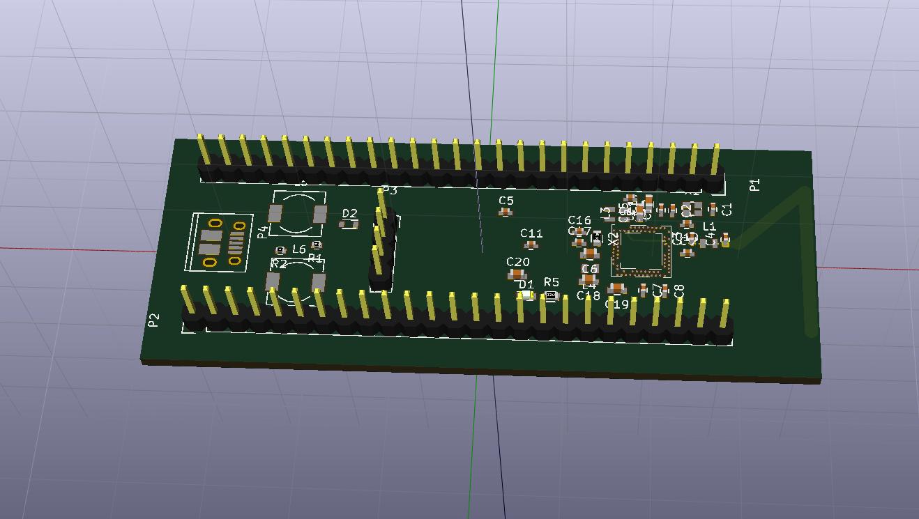
- nrf52840.jpg (84.2 KiB) Viewed 676 times
And I just found that KiCAD can do slot drills and 3D modeling which Eagle cannot for years (esp. slot drills – a real pain)
RogerClark wrote:@racemaniac
I see what you mean about not letting you route anything invalid
Its just the board I’m doing is quite complex and I didnt realise what was going on. Sometimes it let me route tracks and sometimes it didnt
Re: vias without holes
I’ll see if I can convert the altium design reference files as they appear to have a PCB where some SMD pads are via’ed though to a middle layer on a 4 layer board, without a separate via
I’m not sure how that is physically / mechanically achieved
Here are screengrabs from a ref design
Red is the top layer , yellow is a mid layer
The last board I made with KiCad had slots and it worked fine.
Size limitation was probably the main reason I dont use Eagle any more. The 10cm x 10cm limit for the basic commercial version is a pain. Albeit the basic commerical version only cost me $100 USD, but next tier version which allows larger boards was $1000 last time I looked, which IMHO is completely overpriced. I would have probably paid $250 or $500 for larger board capability but not $1000, especially as Eagle is never that easy to use, and for many years looked like. piece of shareware.
With the BGA chip, I contacted the manufacturer / PCB company, and I will need to use 4 layers, but will just use traditional vias under the middle of the BGA, because the nRF52840 only has to rows of pads around the perimeter of the device and there is room under it for the necessary vias. The PCB company can do 0.2mm vias, but I will try to avoid going that small and see if I can use 0.3 or 0.4 and stagger
I decided to use 4 layers because routing from the BGA to the 2 rows of DIL pins e.g. like. Blue Pill was a nightmare on 2 layers and also because the board needs good ground planes as it an RF device as its Bluetooth.
The vias will still go through all layers, hence the ground and power layers will not be absolutely continuous, but I dont think its going to impact the RF performance.
The last board I made with KiCad had slots and it worked fine.
Size limitation was probably the main reason I dont use Eagle any more. The 10cm x 10cm limit for the basic commercial version is a pain. Albeit the basic commerical version only cost me $100 USD, but next tier version which allows larger boards was $1000 last time I looked, which IMHO is completely overpriced. I would have probably paid $250 or $500 for larger board capability but not $1000, especially as Eagle is never that easy to use, and for many years looked like. piece of shareware.
I think 9 mil drills (0.2mm) are pretty standard – should not be too much an increase – and the breakout of BGA needs narrow wires as well.
The fab I used to make my boards last time supports 8mil drills and 5mil wire in their lowest priced bracket.
The fab I used to make my boards last time supports 8mil drills and 5mil wire in their lowest priced bracket.
But I’ve checked and they are OK at 0.2mm vias
And i may be starting to feel the opensource side of KiCad a bit >_<.
I used to work in 4.04, had 4.06 now.
What i’m not so sure about is if anything changed in switching between tools in pbnew, it just felt less smooth than i remembered (i thought pressing escape a few times would completely get me out of the drawing a track tool, but it seems not >_<)
What i am sure about however is that suddenly all my projects defaulted to a solder mask margin of 0.2mm (which is huge on my tiny boards >_<). At first when designing i saw this purple border around my pads that i didn’t seem to recall ever having seen before. When rendering i also saw parts of the tracks bare next to the pads, but thought it was maybe a slight rendering inaccuracy. When checking my gerbers i saw the same problem again, and verified my older gerbers, they were not like that >_<.
So after a bit of googling i found that there is a setting for this solder mask margin, and it somehow was 0.2mm now, set it back to 0 as i had it in the past, but that was a bit of a nasty surprise >_<.
I guess that’s part of using open source software, it’s less consistent in usage, and often a bit less user friendly >_<. The first time i’ve felt KiCad let me down a bit >_<.
I tried Rogers created schematics and symbols libraries for blue pill and ILI9341 SPI + Touch + SD display…
In the schematics mode – it is working just great…with both parts – but when moving into to PCB mode and clicking update PCB from schematics…Kicad complains about that the “Error: Cannot add symbol U3 due to missing footprint BluePill_breakoutst:TJCTM24024-SPI”
So there seems to be some problems here with that symbol…(Even if it is added etc…)
Any great ideas??
Best Regards
Anders
I am fairly knowledgeable regarding KI-Cad and have scripts which are fairly good fixing issues with integrating footprints and 3D model components. Is there a link in the above posts to the Ki-CAD design files for a pill board? Sometimes when I get a mini-board, I have extra space on it. Might be fun to run some off sometime or other.
One limitation of Ki-CAD in my personal use, is that I have to hand edit the insertion of footprint parameters in the project files to adjust orientation and scaling. Most STL editing programs are optimized for game sprite design. A real issue in 3D modeling is world coordinate systems and ground truth. One is dealing with vector abstractions. Game systems and animation are much more forgiving with alignment as it is a visual medium. Floating point numbers are approximations and some minor rounding errors are acceptable.
In EDA and CAD systems where metric and imperial systems are mixed, these rounding errors have consequence. Especially when things are arranged on a grid. So two points may not be exact. In graphics this is part of the dog bone hit area, for rubber banding. This is a region outside the line where there is more area allocated to the end points than the line points. When storing the vectors in the net list, they are stored as vertices in a point cloud. The actual path is an abstraction with multiple solutions. (In 3D these are planes rather than lines.) The order of the vertices can detail the net route.
For some reason (probably because it is confusing to new users.) the digital clay systems work in abstract space. Most of the time this is good enough. You can only zoom into the floating point rounding errors so far. The rest is simply probability and statistics. Why one has to impersonate a demi-goddess from time to time and fix the system manually. Why KI-CAD project files are considered (and according to the doc files designed) to be human readable and editable. (just make a backup before and after.)
a simple schematic a few resistors, 1 transistor, battery, looks alright on the schematic, generate the netlist, use some standard footprints, when it gets to the pcb the netlist is incorrect, connections are broken regardless if i delete and reconnect. maybe there is some bugs in my copy as my installed linux setup is way old easily many years old. my guess is such massive elaborate projects takes time and effort to perfect and certainly more so for open sourced s/w (update:
as it turns out my copies of libraries is so old the transistor has a duplicate pin
https://imgur.com/ZnoROW3
https://imgur.com/WuZ6BPA
fixing that fixed the netlist
a set of some pretty nice youtube video tutorials from digikey i stumbled into:
https://www.youtube.com/watch?v=vaCVh2SAZY4
https://www.youtube.com/watch?v=c2niS9ZRBHo
https://www.youtube.com/watch?v=4Gtd7xY6zS4
https://www.youtube.com/watch?v=ZHH4G_EWhm0
https://www.youtube.com/watch?v=Ghv0bGiZFL8
https://www.youtube.com/watch?v=dM5b_s2ysVk
https://www.youtube.com/watch?v=jaQPr7PgImk
https://www.youtube.com/watch?v=ENmDnoKs2hM
https://www.youtube.com/watch?v=I7GUiGoD1w8
https://www.youtube.com/watch?v=Zkn_Au5aeLA
[Angr77 – Wed Feb 20, 2019 4:19 pm] –
Hi!I tried Rogers created schematics and symbols libraries for blue pill and ILI9341 SPI + Touch + SD display…
In the schematics mode – it is working just great…with both parts – but when moving into to PCB mode and clicking update PCB from schematics…Kicad complains about that the “Error: Cannot add symbol U3 due to missing footprint BluePill_breakoutst:TJCTM24024-SPI”
So there seems to be some problems here with that symbol…(Even if it is added etc…)
Any great ideas??
Best Regards
Anders
Sorry for the confusion…the Kicad library which I refer to is the following: download/file.php?id=2008
The blue pill board works perfect in kicad…but the included symbol/footprint for the 2.4” ili9341 has some problems when moving to PCB mode…
Best regards
Anders

