I have rebuild the Transistor Curve Tracer:
https://www.instructables.com/id/Transi … ve-Tracer/
It was a very nice project from Peter Balch with good documentation and a lot of pictures.
I modified the source a little bit add some new functions and a quicker more simple menu.
Also I add two quad encoders for changing parameters and a better / simpler driver for the DUTs.
The only small problem was , that the Arduino NANO was slow for the SPI-ILI9341 display by changing menu items.
Therefore I tried to migrate the code from Arduino to STMf103 / maple mini.
I have to change a lot, take the code from maddias for the encoders and use SPI_2 for the dual DAC MCP4812.
Instead of the very good graphic library of Peter Balch I have to use the Adafruit_ILI9341_STM, but the fonts are not so good there.
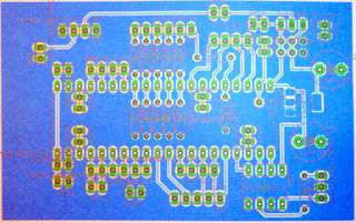
I made a new layout for the “motherboard” for maple-mini, MCP4812 and the 5V LM7805.
On the testsocket I have a double-switch for changing + . (for npn,pnp,…) with a neutral position. In this I can change the DUTs and change the parameters.
Here some pictures from the layot and the Traces from the first DUT (a pnp):
I like it.
I think this will be the next build when I get the other three off the bench.
Thanks for sharing!
(in the video the Icon is wrong!).
https://www.youtube.com/watch?v=VihkScw … e=youtu.be
I think I have enough to do for the next time (from Friyday) !
board backside:
https://www.flickr.com/photos/157863602 … otostream/
board topside with voltage-dividers for adc’s, socket for maplemini, dual-DAC MCP4812, …
https://www.flickr.com/photos/157863602 … otostream/
Board with Maplemini on socket:
https://www.flickr.com/photos/157863602 … otostream/
schematic driver for Uc and UB:
npn:
https://www.youtube.com/watch?v=Vx0zOoM … e=youtu.be
pnp:
[url]https://www.youtube.com/watch?v=lU4GIOO … utu.be[url]n-MOS:
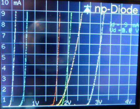
[url]https://www.youtube.com/watch?v=li8PEPm … utu.be[url]now I have a automatic scale selection for Diodes/Zener for the voltage scale. So for small Ud ( schottky , germanium and small planar-diodes) range < 1V, for LED’s smaller 4V and for (most) zener-diodes above (.. 12V):
For JFET’s with IDss <= 10mA the y scale switched from 50mA (max) to 10mA (max):
example nJFET BF244:
https://www.youtube.com/watch?v=HbGsD5e … e=youtu.be
example Diode / Ube:
the scale changed automatically from
12v (for 6.8V Zener voltage ) to 1V (for 0.7V flow voltage).
I think now is the SW nearly ready, next I have to do something with the chassis …
And than I intend to make a video that isn’t so shaky like this:
In the diode-menu in position Max U-Diode = 0 the voltage-range changed automatic to the best/nearest (1V,2V,3V,4V,6V,12V max).
In the j-FET menu the y-scale changed automatic from 50mA to 10mA by small IDss or from 50mA to 100mA to big IDss.
A small demo You can see here:
the switch between n- and p-devices with the double-toggle switch (with neutral/sleep position) made some problems:
– needs space on the small user-surface
– makes longer wires to the ADC’s (more than 6cm)
– was not good usable on the small / light device
– stands often/long time in the wrong / active position and needs power and stressed/heat-up the DUT and the measure-resistances.
Therefore I tested 2 toggle relays for switching, only one active.
Now the DUTs had power only in the short measuring phase,
but I need a relative big PCB and about 70mA/5V for the short active time and a FET/diode and resistance for each relay.
Looking therefore for a electronic switcher and found AQY212: PhotoMOS – Relays
Not so expensive (about 1.5 $ each/I used 4), small , no separate supply but on resistance from about 1 Ohm.
But I think for max. current < 100mA an error from 100mV is – I hope – tolerable.
It works with > 2mA / 1.2V and I need no transistor/FET to drive it.
I need two Pins for activate/deactivate, but it’s functioned very good.
On the menu-screen I have split the “START”-button in two:
“pnp” for start pnp-Transistor, pMOS, n-JFET and p-Diode
“npn” for start npn-Transistor, NMOS, p-JFET and n-Diode
I add new function for comparing one DUT with another on the same screen.
Comparing makes sense with same kinds, for instance one npn with another npn
or with a complementary kind , for instance a npn with a pnp.
Preferably equal/paired transistors/fets you need often , for instance in differential-amplifier inputs.
Paired diodes for instance to select LEDs or zener – diodes.
Paired complementary devices you need for instance in amplifier end-stages.
Normally you start measuring with select the Type: Diode,npn/pnp,MOSFET or JFET and touching the Start-Button “pnp” or “npn”.
For comparing with another Device you change the device on the socket and
— turn the encoder (normally used for increment) CW for the same type (for instance : npn <—> npn
— turn the encoder (normally used for increment) CCW for a complementary type (for instance : npn <—> pnp
The compared device will be painted with another color on the screen.
Another problem was, that there was no current limit (only -I hope – in the amplifier TCA0372).
Therefore I designed a current limit over the measuring resistance (R32/R37 = 100 Ohm) and fixed it to 49mA.
https://www.youtube.com/watch?v=Q7o3SxdtTYw
In the original design from Peter Balch their was onlya pos. supply voltage for the DUT’s. Therefore we had problems with the opamps near 0V , we need a rail-to-rail opamp with more than 100 mA output. I tested some opamps, I think the bestI found were L2272 or TCA0372, but they are no real r-to-r devices.
Also we need negative supply voltage on the gate of nJFETs.
Peter found a trick: he start it in the P-menu (emitter / source on 12V), draw gate to 0V and drain to + supply and the source to output of opamp, voltage varying by SW/DAC.
But therefore you had not the full voltage between source and drain and I think only for small drain-source-voltages the trace
was correct.
Threfore I made with a ICL7662 from the + 13V suppy a negative with more/less than -12V.
I used a separate standard dual opamp, for instance a TL062/072 only for the base. The 1. opamp works “normal” as non-ivertingv and gain 3 (66k/33k), the second opamp for the n-JFET works as inverting Opamp gain -3 (33k/100k).
With an Opto-Mos-Relais AQY212 ![]() I switch between the opamp-outputs to lay + or – voltage/current (over a 27k resistance) on the base.
I switch between the opamp-outputs to lay + or – voltage/current (over a 27k resistance) on the base.
Now the traces are better with less moise and it’s also possible to test depletion-mode MOSFET’s .
They have similar behavior like n-JFET’s, but the traces are very flat.
Instead of TL062 I use a LT1013, because he can work up to 44V and has output-current > 10mA.
The LT1013 has a negative supply (for n-JFET and depletion n_MOSFET) from about 12V (via ICL7662) and a positive supply from about +27V (via MT3608) for driving Zener -Diodes with Vz <= 24V /5mA.
The short video shows the result.
I think it could be the standard-layout for many projects:
it has headers for:
– ILI9341-SPI-TFT (only SCK, MOSI of SPI1 used, CS and CD on Pin 1,2)
– Touch (URTOUCH)
– 6 ADC’s with voltage divider on board
– I2C (SDA.SCLl) Pin 15,16 (I tested it with MCP23017 expander)
– USB (Pin 23,24)
– RX/TX (Pin25,26) for instance for Bluetooth
– 2 encoder over ISR (Pin17,18 and 13,14)
– SPI2 ( usable for instance for dual DAC MCP4822 (DIL8 on board) on Pin 28…31)
– 3 buttons (Pin0,Pin19,Pin20)
– Reset
and a own + 3.3V supply for display,… (I think is good for the internal reference).
and a own – 3,3V/ or -5V supply (for instance for amplifier)
Now the board has the dimension of the 2.8″ ILI9341 display (5cm x 8.5cm)
here the tentative layout:
- MapleMiniCurveTracer_board_01.JPG (18.29 KiB) Viewed 488 times
Integrate the zener-test in the “normal” Diode region, I need no separate socket for zener – diodes.
But therefore I had to change the voltage-dividers on four analog inputs from 100k/33k to 100k/11.??k
by paralleling a 20k to the 33k. Now the max. input voltage is near 30V .
I switch the 20k resistors with four nMOS-Fets.
Behind the “mother-board” for the maple-mini/MCP48x2 I have two small boards, one with the TCA0372 amplifier
for collector/emitter currents, the other with LT1303 to generate base current / gate-voltages.
The supply-voltage for the TCA0372 changed from 12.5V (normal) to 26V for measuring zener – diodes > 12V ,
The LT1303 has a separate supply ( about 27V ), the negative -12V supply for nJFET I generate with a ICL7662 (with a LM317L
for +12v).
Some more hw, but the sw and the handling is clearer.
The test’s are good , I will make a new video if I have finished a new chassis ![]()
I’m following all your progress on this…
and the right edge. And I have more space for a third parameter (most maximal-values) and on the left side the possibility to display all 4×3 parameter-values. Also I integrate the possibility to save the parameters in the EEPROM ( inside the STM32F103/MapleMini).
A short “video” here:
the gain of the amplifier TCA0372 now is changeable from gain=1(for (shottky-)diodes, LED’s and zener with Vz < 4V) over gain = 3 (default) to gain = 6 (for zeners with Vz between 12 and 24V).
Gives better resolution:
here the compare – function:
start on the left with Shottky-Diode, than a 1N4184, RED-LED, YELLOW-LED, GREEN-LED, WHITE-LED
all at max. 9mA. The LED’s are standard 5mm.
- MapleTracer_337_DiodesCompColor-002.JPG (40.23 KiB) Viewed 431 times
now I have finished the work nearly, made some expansions for n-JFET with better resolution:
https://www.youtube.com/watch?v=7slY69G … e=youtu.be
In the next days I will publish it in Github.
now I have put some files in Github.
look here :
I have changed the display for n-/p-JFETs.
You can change the x-scale from 2 to 12V (2,3,4,6,12V).
The display shows two ohmic resistance (angled lines from zero).
The 2V x-scale is good for analyze the ohmic region of the jFETs between 0V and Vpinch.
12V – scale:
https://www.youtube.com/watch?v=IF9O-zO1Lq4
2V – scale:
at 10 mA max:
https://www.youtube.com/watch?v=2wD9CJixKr4
and at 46 mA max:
