TODO:
-Design footprints. Need to decide on a micro USB port and design a few other footprints.
-Finish schematic.
-Hack bootloader(pin mapping, etc.)
-Design the PCB
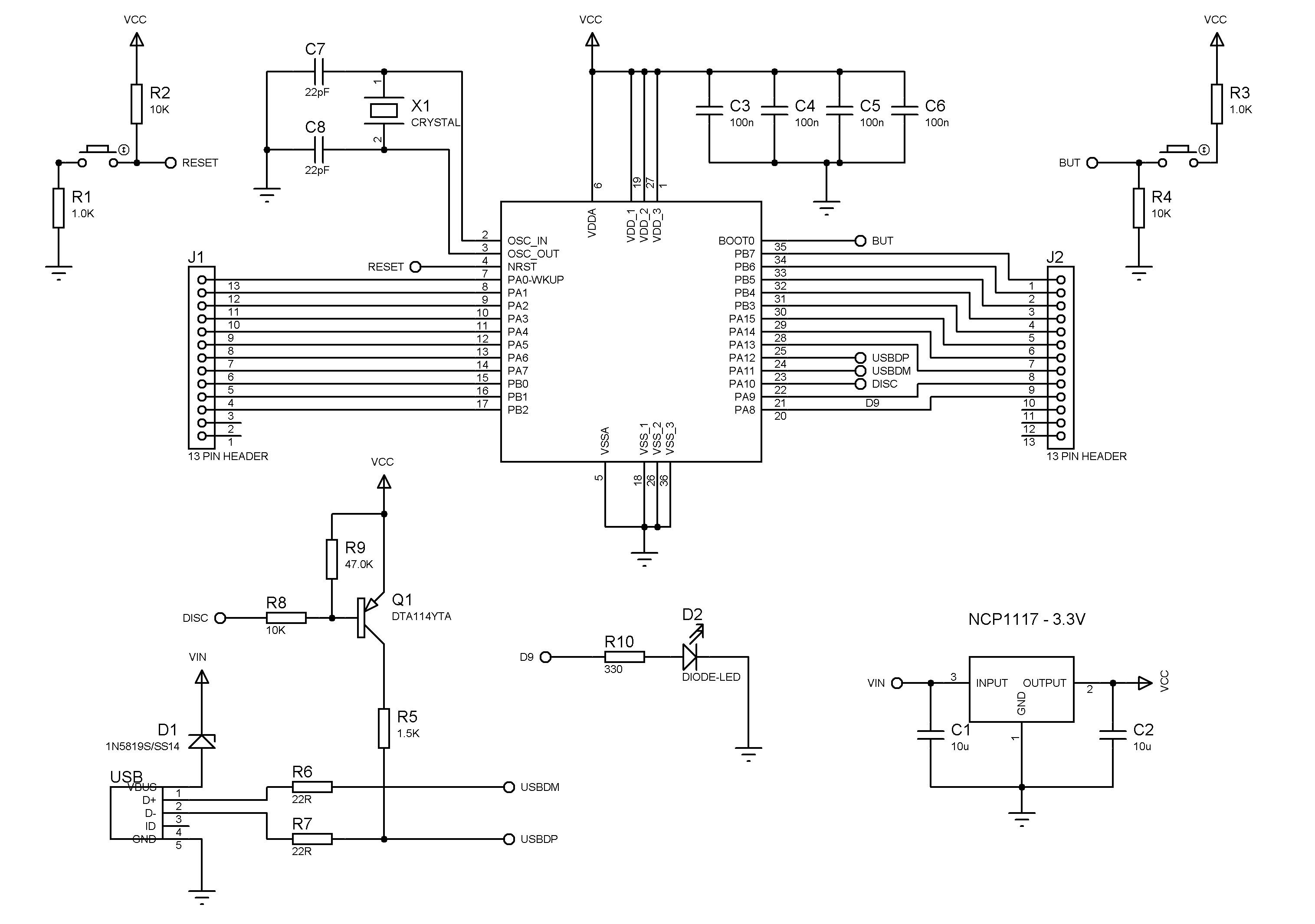
Any thoughts or suggestions are welcome. Here’s the schematic so far. Note that D9(On board LED pin) will most likely change among other things.
<…>
Any thoughts or suggestions are welcome. Here’s the schematic so far. Note that D9(On board LED pin) will most likely change among other things.
That way you remove a few components and dont need to reserve a pin for DISC. We found a way to cause usb enumeration by just toggling PA12, and the stm32duino bootloader and the core include the code. Just select a “generic” board rather than a maple one when compiling.
EDIT:I’m going to read up on the generic bootloader.
EDIT2: Found it. I think I can add the transistor to be sure, though. It’s tiny. Unless you think it’s a waste of time.
On “generic” boards, the USB reset (to force re-enumeration by the host), is triggered by reconfiguring USB line D+ (PA12) into GPIO mode, and driving PA12 low for a short period, before setting the pin back to its USB operational mode. This system to reset the USB was written by @Victor_pv. Note. It is not guaranteed to work on all “generic” STM32 boards, and relies on PA12 having a pull-up resistor of around 1.5k – however most “generic” boards seem to have this. Its unclear if this method to reset the USB bus conforms precisely to the USB standard, but it seems to work fine on all PC’s and Mac’s (and Linux boxes) on which its been tested – and seems usable for hobby / non commericial / non-critical systems.
I had recently started a topic about a Teensy alternative STM32 board using STM32F103C8.
Now I see you have progressed on designing similar board much more ahead than me (I am more focused on my SmartWatch project). It would be great to see such board.
I recommend you to examine STM32F103C8 development boards and schematics (named here as blue pill and red pill) They are my favorite boards since they are very neat, simple designed, commonly used, has small footprint and also compatible with stm32duino with many supported libraries.
Edit: I also found another type of STM32F103T8 board: http://www.artekit.eu/products/devboard … m32-dip36/
Waiting to see some pics
Furkan
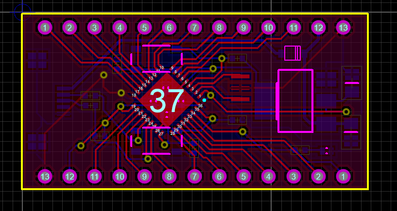
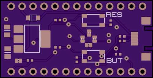
I’m new to electronics in general and don’t have very much time to work on anything, unfortunately. I don’t think I could come up with something professional enough for everyone to use with my current skills. When I first started routing the board I didn’t think I could fit the crystal I had on there, so I switched it to the resonator that I used before. I do have the room for it on the board though, after all, so I’m switching it back. Still needs work and silkscreen.
You’re right those boards are tidy. This is mainly just practice for me. I got the board down to 18x35mm.
I do have the room for it on the board though, after all, so I’m switching it back.
I just double checked everything and sent off to OSHpark. Swapped the resonator for the crystal, finally decided on the USB port and added the silkscreen for pins and switches. These will only be for prototyping for my actual project that I’ll be working on. ![]() I can’t wait to see how the ADC performs, as it could be much better. We’ll just have to see.
I can’t wait to see how the ADC performs, as it could be much better. We’ll just have to see.
EDIT: I just noticed I added the pins silkscreen on actual bottom of the board, as the top and bottom are actually different than how it’ll be on a breadboard. Going to have to be like that for now. I can snap a pic of the pinout and use that.
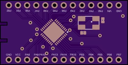
Maybe you could leave off the first letter of each pin name for saving some free space on silkscreen.
Instead of writing “PA1”, “PB3” etc just write “A1” , “B3” (without the quotes).
Also, you could use bigger font size than the font size you already use.
Some silkscreens are not printer very clear on PCB. A bigger font size could help in solving that problem.
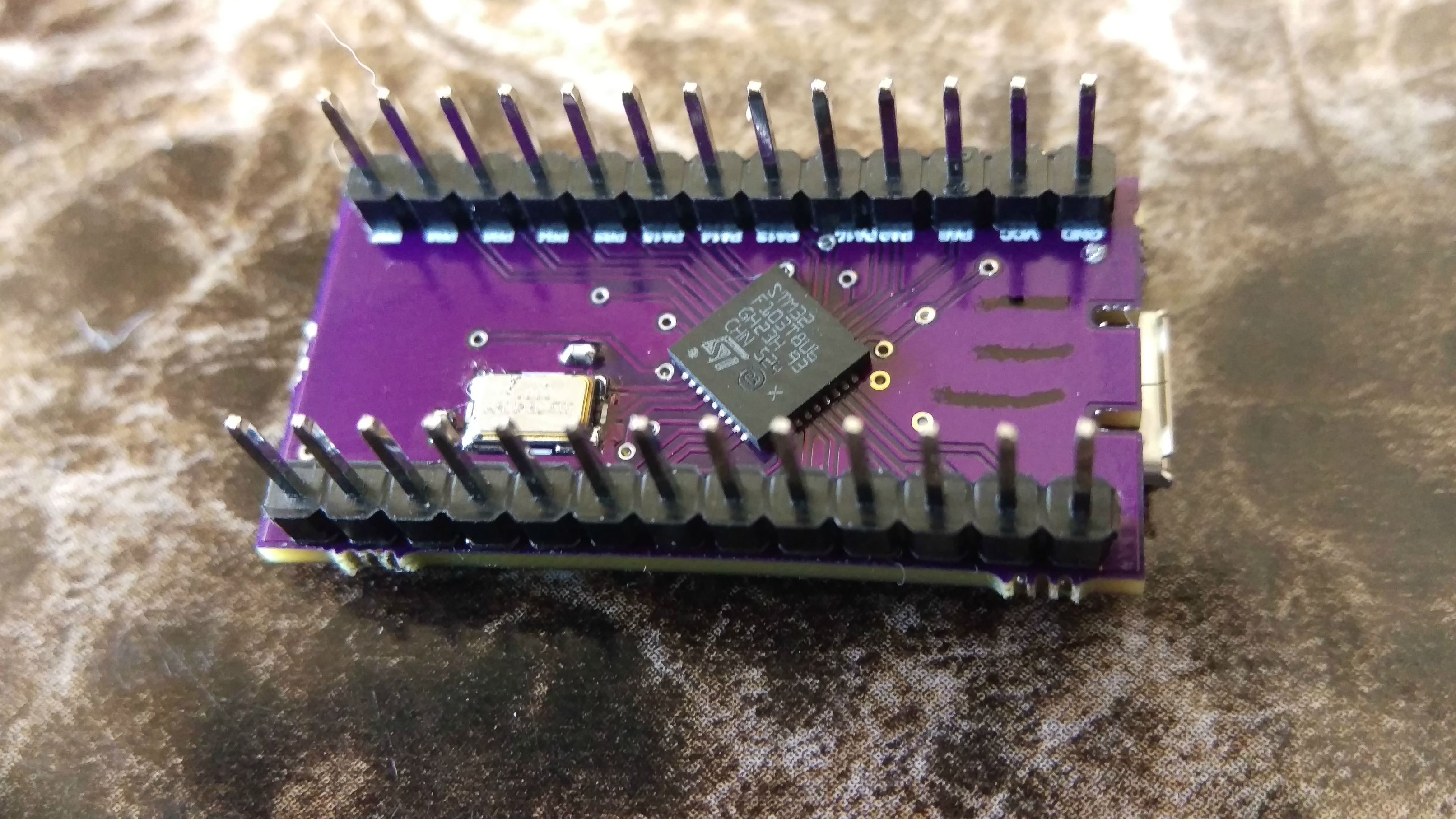
One thing I just spotted, which I wasn’t aware of, according to the STM32F103xx performance line VFQFPN36 pinout, there is no separate VBAT pin for the RTC and backup power domain (correct me if I am wrong).
This means that any battery powered projects will have to use software sleep tricks, exclusively to keep power usage to a minimum if you want to preserve the RTC values for long periods. You can’t simply kill the main battery and rely on a separate RTC battery.
This is not a major issue, as for most low power projects I would expect the design to use the sleep modes as much as possible. Furthermore several of the STM32F103 boards I have, have VBAT linked to VDD anyway. I think ST missed a trick here, as they could have replaced one of the three VDD pins with VBAT. No doubt the ST designers had their reasons.
I really need to check out sleep mode. I haven’t lookd into it at all with these.

proxy i’ve never set one, gmail is bw494540
stephen
proxy i’ve never set one, gmail is bw494540
stephen
One thing I just spotted, which I wasn’t aware of, according to the STM32F103xx performance line VFQFPN36 pinout, there is no separate VBAT pin for the RTC and backup power domain (correct me if I am wrong).
This means that any battery powered projects will have to use software sleep tricks, exclusively to keep power usage to a minimum if you want to preserve the RTC values for long periods. You can’t simply kill the main battery and rely on a separate RTC battery.
This is not a major issue, as for most low power projects I would expect the design to use the sleep modes as much as possible. Furthermore several of the STM32F103 boards I have, have VBAT linked to VDD anyway. I think ST missed a trick here, as they could have replaced one of the three VDD pins with VBAT. No doubt the ST designers had their reasons.
This was my first time with 0402 components as well as QFN. I used a mylar stencil and had issues with the QFN. 0402 and other components weren’t an issue. I’ll let you guys know how the rest of testing goes. Here’s a video for you. I’ve never been happier to see an LED blink. ![]()

May be an option…
May be an option…
I’m hoping to rock the stm32duino bootloader tomorrow and test the ADC. Hoping it’s not too noisy. We shall see.
EDIT: Here’s a comparison to the Teensy 3.1
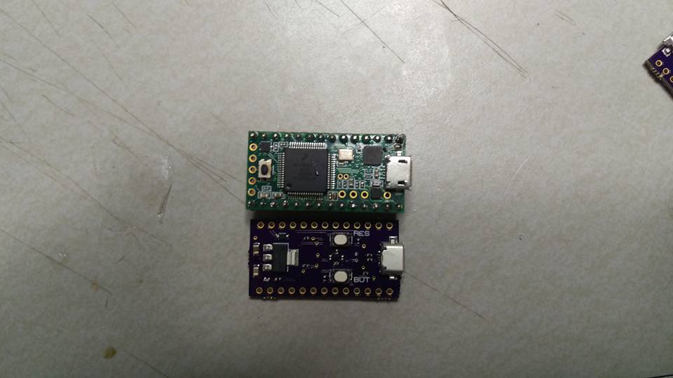
The other difference is which pin the user button is connected to (if you have a user button)
If you look in config.h its fairly easy to see which config would suit you, and if none match, its quite easy to build a new version, or just hack one of the existing configs to meet your needs
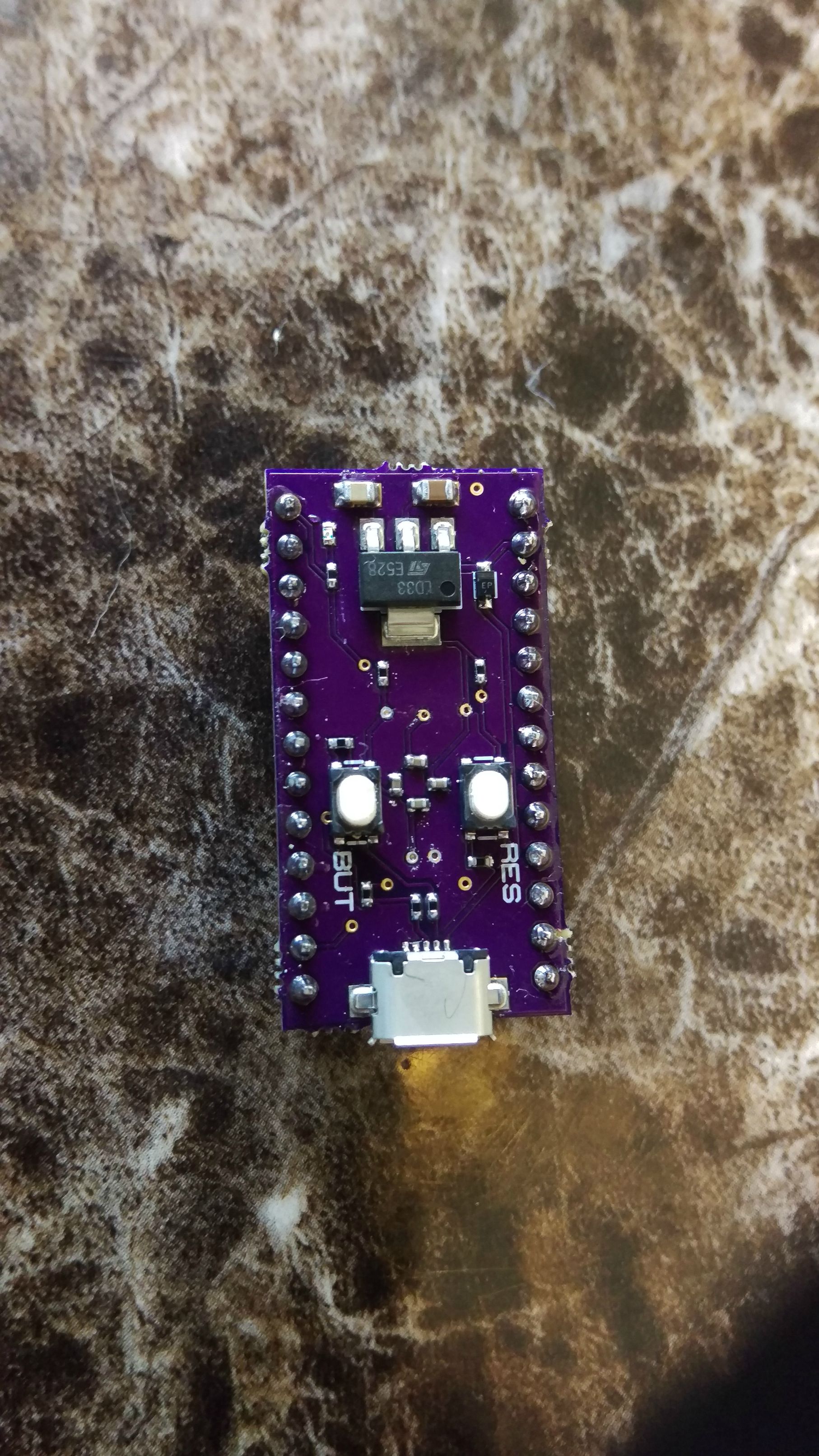
I read in another topic that people were saying they compiled with GCC 4.8.3 and it worked, so I guess that’s my next step. I have the LED on PB7 and only buttons I have on the board are RST and BUT(boot0).
Side note, I had to use PA9/PA10 for UART and pulled PB2(boot1)low manually with a wire to flash the bootloader. The other UART pins weren’t working for me, so I need to test all the pins to make sure they’re OK.
EDIT:I might not have a chance to fix the bootloader anytime soon, as I’m going into a very strenuous work week. Anyone want to compile a generic bootloader for me with LED on PB7 and no extra buttons? I noticed this thread should be in the custom boards section as well, so you can move it if you like. The help with the bootloader would be appreciated, but I can do it eventually.
I just added generic-pb7
It should not have a button
Please test and let me know if it works for you
OK, I tried flashing the one you uploaded and it won’t even flash 100%. It errors out @ 99% and says, “Write address and length must be 4 byte aligned.” I flashed another one just to make sure everything is OK on my end and it flashed 100% OK the first time. Weird, huh?
EDIT:My fault.
I just tried building again, but I get exactly the same bin file.
can you try downloading it again
Github can be a bit confusing, the bin links take you to another page, where you then need to press the RAW button, to get the real file if its a bin
I have two that are working so far with the STM32duino bootloader. One that all pins work except for PA0, PA1 and PA2 and another with every pin working. The funny thing is, the soldering around the two working ones doesn’t look quite as good as the one that would only upload with an STlink programmer. I MCU you can see in the pic is the one that’s not working. I reflowed the crystal(ehh, it looked OK), but wanted to try to get some closeup shots of the board to you show you what it looks like.
I have enough to go on now to continue testing with my project, but I’ll let you guys know how the MCU reflows go.
Side note, here’s how I’m testing the pins. I’m using a jumper to go from the pin I’m testing over to the LED pin(PB7 on this board). I whipped up this sketch that is very simple. Totally works.
byte myPins[] = {PA0,PA1,PA2,PA3,PA4,PA5,PA6,PA7,PA8,PA9,PA10,PA11,PA12,PA13,PA14,PA15,PB0,PB1,PB2,PB3,PB4,PB5,PB6};
void setup() {
for (int i = 0;i <= 22; i++)
pinMode(myPins[i], OUTPUT);
}
void loop() {
for (int i = 0;i <= 22; i++){
digitalWrite(myPins[i], HIGH);
}
delay(250);
for (int i = 0;i <= 22; i++){
digitalWrite(myPins[i], LOW);
}
delay(250);
}


